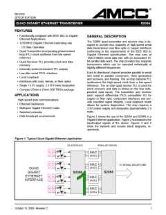
QUAD GIGABIT ETHERNET TRANSCEIVER
TRANSMITTER DESCRIPTION
S2066
The S2066 also provides a system clock output,
TCLKO, which is derived from the internal VCO. The
frequency of this output is constant at the parallel
word rate, 1/10 the serial data rate, regardless of
whether the reference is provided at 1/10 or 1/20 the
serial data rate. This clock can be used by upstream
circuitry as a system clock. See Table 1.
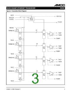
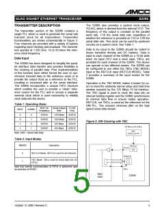
The transmitter section of the S2066 contains a
single PLL which is used to generate the serial rate
transmit clock for all transmitters. Transmitter
functionalities are shown schematically in Figure 3.
Four channels are provided with a variety of options
regarding input clocking and loopback. The transmit-
ters operate at 1.250 GHz, 10 or 20 times the refer-
ence clock frequency.
Data to be input to the S2066 should be coded to
insure transition density and DC balance. Data is
input to each channel of the S2066 as a 10 bit wide
word. An input FIFO and a clock input, TBCx, are
provided for each channel of the S2066. The device
can operate in two different modes. The S2066 can
be configured to use either the TBCx (TBC MODE)
input or the REFCLK input (REFCLK MODE). Table
2 provides a summary of the input modes for the
S2066.
Data Input
The S2066 has been designed to simplify the paral-
lel interface data transfer and provides flexibility in
the clocking of parallel data. Prior implementations
of this function have either forced the user to syn-
chronize transmit data to the reference clock or to
provide the output clock as a reference to the PLL,
resulting in increased jitter at the serial interface.
The S2066 incorporates a unique FIFO structure
which enables the user to provide a “clean” refer-
ence source for the PLL and to accept a separate
external clock which is used exclusively to reliably
clock data into the device.
Operation in the TBC MODE makes it easier for us-
ers to meet the relatively narrow setup and hold time
window required by the 125 Mbps 10 bit interface.
The TBC signal is used to clock the data into an
internal holding register and the S2066 synchronizes
its internal data flow to ensure stable operation.
REFCLK, not TBCx, is used as the reference for the
DIN PLL. This ensures minimum jitter on the high
speed serial data stream.
Table 1. Operating Rates
REFCLK
Frequency
Serial Output
Rate
TCLK0
Freq
RATE
CLKSEL
0
0
1
1
0
1
0
1
SDR/10
SDR/20
SDR/10
SDR/20
1250 Mbps
1250 Mbps
625 Mbps
625 Mbps
SDR/10
SDR/10
SDR/10
SDR/10
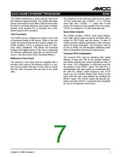
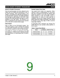
Figure 5. DIN Clocking with TBC
125 MHz or 62.5 MHz
REF
OSCILLATOR
Note: SDR = Serial Data Rate.
Table 2. Input Modes
TMODE
Operation
REFCLK
TCLKO
PLL
0
1
REFCLK Mode. REFCLK used for all channels.
DINx[0:9]
TBC Mode. TBCx used to clock data into all
FIFOs.
Note that internal synchronization of FIFOs is performed upon
de-assertion of RESET.
TBCx
MAC
S2066
ASIC
5
October 13, 2000 / Revision C

 AMCC [ APPLIED MICRO CIRCUITS CORPORATION ]