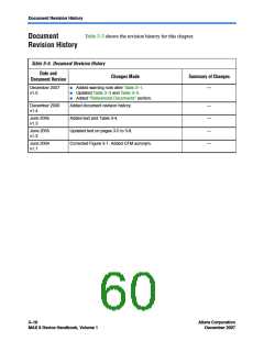
JTAG and In-System Programmability
Design Security
All MAX II devices contain a programmable security bit that controls
access to the data programmed into the CFM block. When this bit is
programmed, design programming information, stored in the CFM
block, cannot be copied or retrieved. This feature provides a high level of
design security because programmed data within flash memory cells is
invisible. The security bit that controls this function, as well as all other
programmed data, is reset only when the device is erased. The SRAM is
also invisible and cannot be accessed regardless of the security bit setting.
The UFM block data is not protected by the security bit and is accessible
through JTAG or logic array connections.
Programming with External Hardware
MAX II devices can be programmed by downloading the information via
®
in-circuit testers, embedded processors, the Altera ByteblasterMV™,
MasterBlaster™, ByteBlaster™ II, and USB-Blaster cables.
BP Microsystems, System General, and other programming hardware
manufacturers provide programming support for Altera devices. Check
their websites for device support information.
This chapter references the following documents:
Referenced
Documents
■
■
■
■
DC and Switching Characteristics chapter in the MAX II Device
Handbook
IEEE 1149.1 (JTAG) Boundary-Scan Testing for MAX II Devices
chapter in the MAX II Device Handbook
Real-Time ISP and ISP Clamp for MAX II Devices chapter in the
MAX II Device Handbook
Using Jam STAPL for ISP via an Embedded Processor chapter in the
MAX II Device Handbook
Altera Corporation
December 2007
Core Version a.b.c variable
3–9
MAX II Device Handbook, Volume 1

 ALTERA [ ALTERA CORPORATION ]