Introduction to the Stratix GX Device Data Sheet
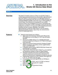
Figure 1–1. Stratix GX I/O Blocks
Note (1)
DQST9 DQST8 DQST7 DQST6 DQST5
DQST4 DQST3 DQST2 DQST1 DQST0
VREF1B4 VREF2B4 VREF3B4 VREF4B4 VREF5B4
Bank 4
PLL5
PLL7 VREF1B3 VREF2B3 VREF3B3 VREF4B3 VREF5B3
Bank 3
PLL11
9
10
I/O Bank 13 (5)
LVDS, LVPECL, 3.3-V PCML,
and HyperTransport I/O Block
and Regular I/O Pins (3)
(4)
I/O Banks 3, 4, 9 & 10 Support
All Single-Ended I/O Standards (2)
I/O Bank 14 (5)
I/O Bank 17 (5)
I/O Banks 1 and 2 Support All
Single-Ended I/O Standards Except
Differential HSTL Output Clocks,
Differential SSTL-2 Output Clocks,
HSTL Class II, GTL, SSTL-18 Class II,
PCI, PCI-X, and AGP 1×/2×
PLL1
PLL2
1.5-V PCML (5)
I/O Bank 16 (5)
I/O Bank 15 (5)
I/O Banks 7, 8, 11 & 12 Support
All Single-Ended I/O Standards (2)
(4)
LVDS, LVPECL, 3.3-V PCML,
and HyperTransport I/O Block
and Regular I/O Pins (3)
Bank 8
11
12
Bank 7
VREF5B8 VREF4B8 VREF3B8 VREF2B8 VREF1B8
DQSB9 DQSB8 DQSB7 DQSB6 DQSB5
PLL12
VREF5B7 VREF4B7 VREF3B7 VREF2B7 VREF1B7
DQSB4 DQSB3 DQSB2 DQSB1 DQSB0
PLL8
PLL6
Notes to Figure 1–1:
(1) Figure 1–1 is a top view of the Stratix GX silicon die.
(2) Banks 9 through 12 are enhanced PLL external clock output banks.
(3) If the high-speed differential I/O pins are not used for high-speed differential signaling, they can support all of the
I/O standards except HSTL class I and II, GTL, SSTL-18 Class II, PCI, PCI-X, and AGP 1×/2×.
(4) For guidelines for placing single-ended I/O pads next to differential I/O pads, see the Selectable I/O Standards in
Stratix & Stratix GX Devices chapter of the Stratix GX Device Handbook, Volume 2.
(5) These I/O banks in Stratix GX devices also support the LVDS, LVPECL, and 3.3-V PCML I/O standards on
reference clocks and receiver input pins (AC coupled).
Stratix GX devices contain a two-dimensional row- and column-based
architecture to implement custom logic. A series of column and row
interconnects of varying length and speed provide signal interconnects
between logic array blocks (LABs), memory block structures, and DSP
blocks.
FPGA Functional
Description
Altera Corporation
February 2005
1–5
Stratix GX Device Handbook, Volume 1

 ALTERA [ ALTERA CORPORATION ]