TriMatrix Memory
You cannot use an initialization file to initialize the contents of a M-RAM
block. All M-RAM block contents power up to an undefined value. Only
synchronous operation is supported in the M-RAM block, so all inputs
are registered. Output registers can be bypassed.
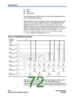
Similar to all RAM blocks, M-RAM blocks can have different clocks on
their inputs and outputs. Either of the two clocks feeding the block can
clock M-RAM block registers (renwe, address, byte enable, datain,
and output registers). The output register can be bypassed. The six
labclksignals or local interconnect can drive the control signals for the
A and B ports of the M-RAM block. ALMs can also control the clock_a,
clock_b, renwe_a, renwe_b, clr_a, clr_b, clocken_a, and
clocken_bsignals, as shown in Figure 2–46.
Figure 2–46. M-RAM Block Control Signals
Dedicated
Row LAB
6
Clocks
Local
Local
Interconnect
Interconnect
Local
Local
Interconnect
Interconnect
Local
Local
Interconnect
Interconnect
Local
Local
Interconnect
Interconnect
Local
Local
Interconnect
Interconnect
clocken_a
renwe_a
clock_b
aclr_b
Local
Interconnect
Local
Interconnect
clocken_b
clock_a
aclr_a
renwe_b
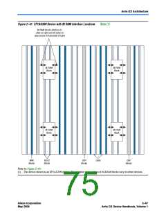
The R4, R24, C4, and direct link interconnects from adjacent LABs on
either the right or left side drive the M-RAM block local interconnect. Up
to 16 direct link input connections to the M-RAM block are possible from
the left adjacent LABs and another 16 are possible from the right adjacent
LAB. M-RAM block outputs can also connect to left and right LABs
through direct link interconnect. Figure 2–47 shows an example floorplan
for the EP1AGX90 device and the location of the M-RAM interfaces.
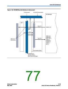
Figures 2–48 and 2–49 show the interface between the M-RAM block and
the logic array.
2–66
Arria GX Device Handbook, Volume 1
Altera Corporation
May 2008

 ALTERA [ ALTERA CORPORATION ]