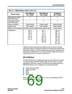
TriMatrix Memory
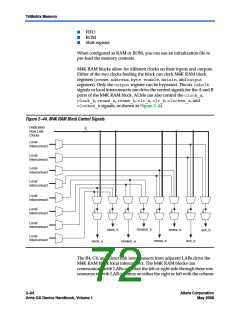
M512 RAM blocks can have different clocks on its inputs and outputs.
The wren, datain, and write address registers are all clocked together
from one of the two clocks feeding the block. The read address, rden, and
output registers can be clocked by either of the two clocks driving the
block, allowing the RAM block to operate in read and write or input and
output clock modes. Only the output register can be bypassed. The six
labclksignals or local interconnect can drive the inclock, outclock,
wren, rden, and outclrsignals. Because of the advanced interconnect
between the LAB and M512 RAM blocks, ALMs can also control the wren
and rdensignals and the RAM clock, clock enable, and asynchronous
clear signals. Figure 2–42 shows the M512 RAM block control signal
generation logic.
Figure 2–42. M512 RAM Block Control Signals
Dedicated
6
Row LAB
Clocks
Local
Interconnect
Local
Interconnect
Local
Interconnect
Local
Interconnect
Local
Interconnect
Local
Interconnect
Local
Interconnect
outclocken
inclocken
wren
Local
Interconnect
outclr
inclock
outclock
rden
The RAM blocks in Arria GX devices have local interconnects to allow
ALMs and interconnects to drive into RAM blocks. The M512 RAM block
local interconnect is driven by the R4, C4, and direct link interconnects
from adjacent LABs. The M512 RAM blocks can communicate with LABs
on either the left or right side through these row interconnects or with
LAB columns on the left or right side with the column interconnects. The
2–62
Arria GX Device Handbook, Volume 1
Altera Corporation
May 2008

 ALTERA [ ALTERA CORPORATION ]