Arria GX Architecture
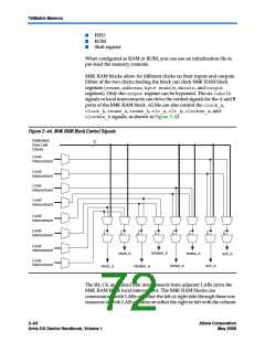
M512 RAM block has up to 16 direct link input connections from the left
adjacent LABs and another 16 from the right adjacent LAB. M512 RAM
outputs can also connect to left and right LABs through direct link
interconnect. The M512 RAM block has equal opportunity for access and
performance to and from LABs on either its left or right side. Figure 2–43
shows the M512 RAM block to logic array interface.
Figure 2–43. M512 RAM Block LAB Row Interface
C4 Interconnect
R4 Interconnect
16
Direct link
Direct link
interconnect
to adjacent LAB
interconnect
to adjacent LAB
36
dataout
M4K RAM
Block
Direct link
Direct link
interconnect
interconnect
from adjacent LAB
from adjacent LAB
datain
byte
enable
control
signals
clocks
address
6
M4K RAM Block Local
Interconnect Region
LAB Row Clocks
M4K RAM Blocks
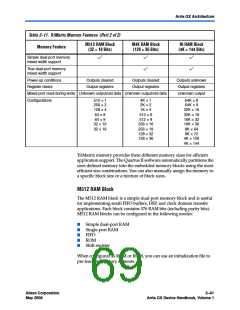
The M4K RAM block includes support for true dual-port RAM. The M4K
RAM block is used to implement buffers for a wide variety of applications
such as storing processor code, implementing lookup schemes, and
implementing larger memory applications. Each block contains
4,608 RAM bits (including parity bits). M4K RAM blocks can be
configured in the following modes:
■
■
■
True dual-port RAM
Simple dual-port RAM
Single-port RAM
Altera Corporation
May 2008
2–63
Arria GX Device Handbook, Volume 1

 ALTERA [ ALTERA CORPORATION ]