Configuration and Testing
1
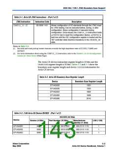
Arria GX, Stratix®, Stratix II, Stratix GX, Stratix II GX,
Cyclone® II, and Cyclone devices must be within the first 17
devices in a JTAG chain. All of these devices have the same JTAG
controller. If any of the Stratix, Arria GX, Cyclone, and
Cyclone II devices are in the 18th or further position, they will
fail configuration. This does not affect the functionality of the
SignalTap II embedded logic analyzer.
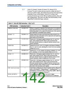
Table 3–1. Arria GX JTAG Instructions (Part 1 of 2)
JTAG Instruction
Instruction Code
Description
00 0000 0101
Allows a snapshot of signals at the device pins to be captured
and examined during normal device operation and permits an
initial data pattern to be output at the device pins. Also used by
the SignalTap II embedded logic analyzer.
SAMPLE/PRELOAD
00 0000 1111
11 1111 1111
Allows external circuitry and board-level interconnects to be
tested by forcing a test pattern at the output pins and capturing
test results at the input pins.
EXTEST (1)
BYPASS
Places the 1-bit bypass register between the TDIand TDO
pins, which allows the BST data to pass synchronously
through selected devices to adjacent devices during normal
device operation.
00 0000 0111
USERCODE
Selects the 32-bit USERCODEregister and places it between
the TDIand TDOpins, allowing the USERCODEto be serially
shifted out of TDO.
00 0000 0110
00 0000 1011
IDCODE
Selects the IDCODEregister and places it between TDIand
TDO, allowing IDCODEto be serially shifted out of TDO.
HIGHZ (1)
Places the 1-bit bypass register between the TDIand TDO
pins, which allows the BST data to pass synchronously
through selected devices to adjacent devices during normal
device operation, while tri-stating all of the I/O pins.
00 0000 1010
CLAMP (1)
Places the 1-bit bypass register between the TDIand TDO
pins, which allows the BST data to pass synchronously
through selected devices to adjacent devices during normal
device operation while holding I/O pins to a state defined by
the data in the boundary-scan register.
—
Used when configuring an Arria GX device via the JTAG port
with a USB-Blaster™, MasterBlaster™, ByteBlasterMV™, or
ByteBlaster II download cable, or when using a .jam or .jbc via
ICR instructions
PULSE_NCONFIG
an embedded processor or JRunnerTM
.
00 0000 0001
Emulates pulsing the nCONFIGpin low to trigger
reconfiguration even though the physical pin is unaffected.
3–2
Altera Corporation
May 2008
Arria GX Device Handbook, Volume 1

 ALTERA [ ALTERA CORPORATION ]