On-Chip Termination
the external 50- resistors connected to the RUPand RDNpins and
dynamically enables or disables the transistors until they match.
Calibration happens at the end of the device configuration. Once the
calibration circuit finds the correct impedance, it powers down and stops
changing the characteristics of the drivers.
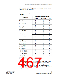
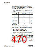
Table 4–7. Selectable I/O Drivers with On-Chip Parallel Termination with
Calibration
On-Chip Parallel Termination Setting
I/O Standard
Unit
(Column I/O)
SSTL-2 Class I
50
50
50
50
50
50
50
50
50
SSTL-2 Class II
SSTL-18 Class I
SSTL-18 Class II
1.8-V HSTL Class I
1.8-V HSTL Class II
1.5-V HSTL Class I
1.5-V HSTL Class II
1.2-V HSTL (1)
Note to Table 4–7:
(1) 1.2-V HSTL is only supported in I/O banks 4,7, and 8.
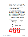
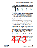
There are two separate sets of calibration circuits in the Stratix II and
Stratix II GX devices:
■
■
One calibration circuit for top banks 3 and 4
One calibration circuit for bottom banks 7 and 8
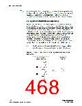
Calibration circuits rely on the external pull-up reference resistor (RUP
)
and pull-down reference resistor (RDN) to achieve accurate on-chip series
and parallel termination. There is one pair of RUPand RDNpins in bank 4
for the calibration circuit for top I/O banks 3 and 4. Similarly, there is one
pair of RUPand RDNpins in bank 7 for the calibration circuit for bottom
I/O banks 7 and 8. Two banks share the same calibration circuitry, so they
must have the same VCCIO voltage if both banks enable on-chip series or
parallel termination with calibration. If banks 3 and 4 have different VCCIO
voltages, only bank 4 can enable on-chip series or parallel termination
with calibration because the RUPand RDNpins are located in bank 4.
Bank 3 still can use on-chip series termination, but without calibration.
The same rule applies to banks 7 and 8.
4–32
Stratix II Device Handbook, Volume 2
Altera Corporation
January 2008

 ALTERA [ ALTERA CORPORATION ]