September 2005
ASM5P23S08A
rev 1.4
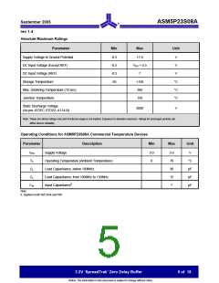
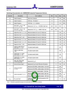
Absolute Maximum Ratings
Parameter
Min
Max
Unit
Supply Voltage to Ground Potential
DC Input Voltage (Except REF)
DC Input Voltage (REF)
-0.5
-0.5
-0.5
-65
+7.0
VDD + 0.5
7
V
V
V
Storage Temperature
+150
260
°C
°C
°C
Max. Soldering Temperature (10 sec)
Junction Temperature
150
Static Discharge Voltage
(As per JEDEC STD22- A114-B)
2000
V
Note: These are stress ratings only and functional usage is not implied. Exposure to absolute maximum ratings for prolonged periods can
affect device reliability.
Operating Conditions for ASM5P23S08A Commercial Temperature Devices
Parameter
Description
Min
Max
Unit
VDD
TA
Supply Voltage
3.0
0
3.6
70
30
15
7
V
Operating Temperature (Ambient Temperature)
Load Capacitance, below 100MHz
Load Capacitance, from 100MHz to 133MHz
Input Capacitance6
°C
pF
pF
pF
CL
CL
CIN
Note:
6. Applies to both Ref Clock and FBK.
3.3V ‘SpreadTrak’ Zero Delay Buffer
5 of 18
Notice: The information in this document is subject to change without notice.

 ALSC [ ALLIANCE SEMICONDUCTOR CORPORATION ]