September 2005
ASM5P23S08A
rev 1.4
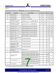
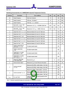
Switching Characteristics for ASM5I23S08 Industrial Temperature Devices
Parameter
Description
Output Frequency
Test Conditions
Min
Typ
Max
Unit
1/t1
1/t1
1/t1
30pF load, All devices
15
15
15
100
133
133
MHz
MHz
MHz
Output Frequency
Output Frequency
15pF load, -5H devices 8
15pF load, -2, -3, -4 devices
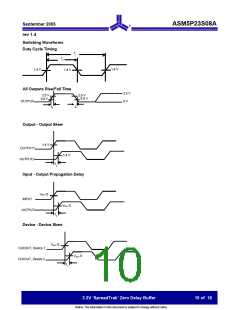
Duty Cycle11 = (t2 / t1) * 100
( -2, -3, -4, -1H, -5H)
Measured at 1.4V, FOUT = <66.66MHz 30pF load
Measured at 1.4V, FOUT = <50MHz 15pF load
40.0
45.0
50.0
50.0
60.0
55.0
%
%
Duty Cycle11 = (t2 / t1) * 100
( -2, -3, -4, -1H, -5H)
t3
t3
t3
t4
t4
t4
Output Rise Time11 ( -2, -3, -4)
Output Rise Time11 ( -2, -3, -4)
Output Rise Time11 ( -5H)
Measured between 0.8V and 2.0V 30pF load
Measured between 0.8V and 2.0V 15pF load
Measured between 0.8V and 2.0V 30pF load
Measured between 2.0V and 0.8V 30pF load
Measured between 0.8V and 2.0V 15pF load
Measured between 2.0V and 0.8V 30pF load
2.50
1.50
1.50
2.50
1.50
1.25
nS
nS
nS
nS
nS
nS
Output Fall Time11 ( -2, -3, -4)
Output Fall Time11 ( -2, -3, -4)
Output Fall Time11 ( -5H)
Output-to-output skew on
same bank ( -2, -3, -4)11
All outputs equally loaded
All outputs equally loaded
All outputs equally loaded
All outputs equally loaded
Measured at VDD /2
200
200
200
400
±250
Output-to-output skew
( -5H)
t5
pS
Output bank A -to- output
bank B skew ( -4, -5H)
Output bank A -to- output
bank B skew (-2, -3)
Delay, REF Rising Edge
to FBK Rising Edge11
t6
t7
0
0
pS
pS
Device-to-Device Skew11
Measured at VDD/2 on the FBK pins of the device
Measured at 66.67MHz, loaded outputs, 15 pF load
Measured at 66.67MHz, loaded outputs, 30 pF load
Measured at 133MHz, loaded outputs, 15 pF load
Measured at 66.67MHz, loaded outputs, 30pF load
Measured at 66.67MHz, loaded outputs, 15pF load
700
200
200
100
400
400
Cycle-to-cycle jitter11
( -4, -5H)
tJ
pS
tJ
Cycle-to-cycle jitter11 (-2, -3)
PLL Lock Time11
pS
Stable power supply, valid clock presented on REF
and FBK pins
tLOCK
1.0
mS
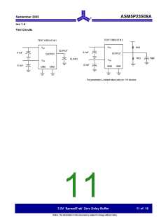
Note: 11. Parameter is guaranteed by design and characterization. Not 100% tested in production.
3.3V ‘SpreadTrak’ Zero Delay Buffer
9 of 18
Notice: The information in this document is subject to change without notice.

 ALSC [ ALLIANCE SEMICONDUCTOR CORPORATION ]