September 2005
rev 1.4
ASM5P23S08A
‘SpreadTrak’
significant amount of tracking skew which may cause
problems in the systems requiring synchronization.
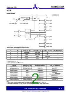
Many systems being designed now utilize a technology
called Spread Spectrum Frequency Timing Generation.
ASM5P23S08A is designed so as not to filter off the
Spread Spectrum feature of the Reference input, assuming
it exists. When a zero delay buffer is not designed to pass
the Spread Spectrum feature through, the result is a
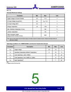
Zero Delay and Skew Control
All outputs should be uniformly loaded to achieve Zero
Delay between input and output.
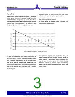
1500
1000
500
0
5
-25
10
25
30
-30
-15
15
20
-20
-10
-5
0
-500
-1000
-1500
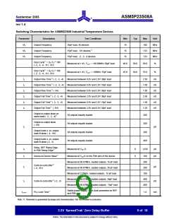
Output Load Difference: FBK Load - CLKA/CLKB Load (pF)
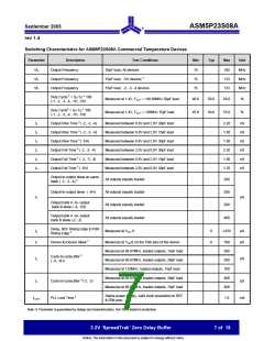
For applications requiring zero input-output delay, all
outputs including the one providing feedback should be
equally loaded. If input-output delay adjustments are
required, use the above graph to calculate loading
differences between the feedback output and remaining
outputs. For zero output-output skew, make sure to load
outputs equally.
To close the feedback loop of the ASM5P23S08A, the FBK
pin can be driven from any of the eight available output
pins. The output driving the FBK pin will be driving a total
load of 7pF plus any additional load that it drives. The
relative loading of this output (with respect to the remaining
outputs) can adjust the input output delay. This is shown in
the above graph.
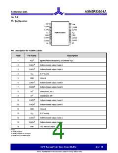
3.3V ‘SpreadTrak’ Zero Delay Buffer
3 of 18
Notice: The information in this document is subject to change without notice.

 ALSC [ ALLIANCE SEMICONDUCTOR CORPORATION ]