Isolated, Digital Output, Power Monitoring IC
with Zero-Crossing Detection, Overcurrent and Overvoltage Flagging
ACS37800
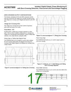
CONFIGURING THE DEVICE FOR DC APPLICATIONS
OR FOR APPLICATIONS WITH NO VOLTAGE ZERO CROSSING
The follow recommendations are provided for DC applications,
value, which is set using EERPOM field n. See the Register
as well as any other applications where there is no voltage zero
crossing. Possible applications include current sensing only,
sensing of a rectified voltage signal, or applications where the
nominal frequency on the voltage channel is greater than 300 Hz.
Details – EEPROM section for additional details.
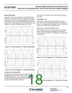
Voltage Measurement
RECOMMENDED APPLICATION CIRCUITS
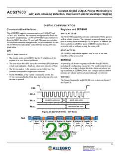
Device EEPROM Settings
The recommended application circuit for the voltage channel in
DC operation is the same as the AC application circuit where
Device GND is connected to Neutral (refer to Figure 17).
For DC power monitoring applications using the ACS37800 or
applications only using the current measurement capability of the
ACS37800, the following device settings are recommended.
Current Measurement
FIXED SETTING OF N
The same considerations for AC applications can be used for the
current path for DC applications.
Set bypass_n_en = 1. This setting disables the dynamic calcula-
tion of n based off voltage zero crossings and sets n to a fixed
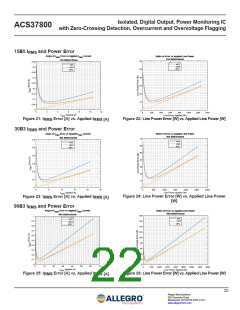
RMS AND POWER ACCURACY VS. OPERATION POINT
RMS and Power Output Error vs. Applied
Input
When using the ACS37800 to measure for RMS calculations and
power monitoring, it is important to consider the error specifica-
tions of the device.
For DC applications, the impact of offset and gain error on the
final output is straightforward, but for RMS and power calcula-
tions, the impact of any errors, specifically offset errors, becomes
dependent on the magnitude of the applied signal.
Figure 20 shows an example system where the maximum measur-
able power is ~1.3 kW, based on the system design. The over-
temperature offset performance of the ACS37800 causes an error
in the measured power that is larger when the applied power is
close to 0 W.
Figure 20: Measured Line Power [W] vs. Applied Line
Power, 15B5 Device
The offset performance of the voltage channel is such that its
contribution to this error is negligible. The current RMS measure-
ment and the power calculations are where this error is observed.
The following figures (Figure 21 through Figure 26) display the
measurement error for the RMS current and active power for
each available device variant.
21
Allegro MicroSystems
955 Perimeter Road
Manchester, NH 03103-3353 U.S.A.
www.allegromicro.com

 ALLEGRO [ ALLEGRO MICROSYSTEMS ]