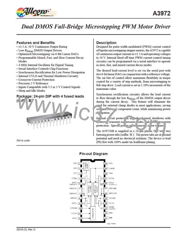
Dual DMOS Full-Bridge
Microstepping PWM Motor Driver
A3972
APPLICATIONS INFORMATION
Current Sensing. To minimize inaccuracies in sensing the
IPEAK current level caused by ground-trace IR drops, the sense
resistor should have an independent ground return to the ground
terminal of the device. For low-value sense resistors, the IR
drops in the sense resistor’s PCB traces can be significant and
should be taken into account. The use of sockets should be
avoided as they can introduce variation in RS due to their contact
resistance.
Layout. The printed wiring board should use a heavy ground
plane. For optimum electrical and thermal performance, the
driver should be soldered directly onto the board. The ground
side of RS should have an individual path to the ground pin(s) of
the driver. This path should be as short as physically possible
and should not have any other components connected to it. The
load supply pin, VBB, should be decoupled with an electrolytic
capacitor (>47 μF is recommended) placed as close to the driver
as is possible.
Thermal Protection. Circuitry turns off all drivers when the
junction temperature reaches 165°C typically. It is intended
only to protect the device from failures due to excessive junction
temperature and should not imply that output short circuits are
permitted. Thermal shutdown has a hysteresis of approximately
15°C.
Serial Port Write Timing Operation. Data is clocked into
a shift register on the rising edge of CLOCK signal. Normally,
STROBE will be held high, and only will be brought low to
initiate a write cycle. The data is written MSB first, followed
by the word-select bit. Refer to serial port diagram for timing
requirements.
SLEEP
H
STROBE
E
C
D
F
G
CLOCK
DATA
A
B
D18
D17
D0
Dwg. WP-038-1
A. Minimum Data Setup Time.......................................15 ns
B. Minimum Data Hold Time ........................................10 ns
C. Minimum Setup Strobe to Clock Rising Edge........150 ns
D. Minimum Clock High Pulse Width...........................40 ns
E. Minimum Clock Low Pulse Width............................40 ns
F. Minimum Setup Clock Rising Edge to Strobe...........50 ns
G. Minimum Strobe Pulse Width.................................150 ns
H. Minimum Setup Sleep to Strobe Falling...................50 μs
Allegro MicroSystems, LLC
115 Northeast Cutoff
9
Worcester, Massachusetts 01615-0036 U.S.A.
1.508.853.5000; www.allegromicro.com

 ALLEGRO [ ALLEGRO MICROSYSTEMS ]