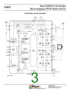
Dual DMOS Full-Bridge
Microstepping PWM Motor Driver
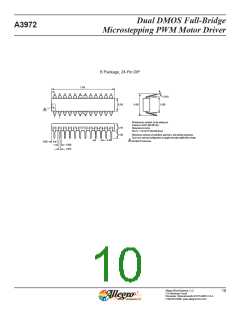
A3972
FUNCTIONAL DESCRIPTION (continued)
Word 1 Bit Assignments
For example, with a master oscillator frequency of 4 MHz, the
fixed off-time will be adjustable from 1.75 μs to 63.75 μs in
increments of 2 μs.
Bit
Function
D0
D1
D2
D3
Word select = 1
Blank-time LSB
Blank-time MSB
Off-time LSB
D8 – D11 Fast Decay Time. These four bits set the fast-
decay portion of fixed off-time for the internal PWM control
circuitry. The fast-decay portion is defined by:
D4
D5
D6
Off-time bit 1
Off-time bit 2
Off-time bit 3
tfd = [(1 + N) x 8/fOSC] - 1/fOSC
where N = 0….15
For example, with an oscillator frequency of 4 MHz, the fast-
decay time will be adjustable from 1.75 μs to 31.75 μs in incre-
ments of 2 μs. For tfd > toff , the device will effectively operate
in fast-decay mode.
D7
D8
D9
Off-time MSB
Fast-decay time LSB
Fast-decay time bit 1
Fast-decay time bit 2
Fast-decay time MSB
C0 oscillator control
C1 oscillator control
SR control bit 1
SR control bit 2
Reserved for testing
Reserved for testing
Idle mode
D10
D11
D12
D13
D14
D15
D16
D17
D18
D12 – D13 Oscillator Control. A 4 MHz internal oscillator
is used for the timing functions and charge-pump clock. If more
precise control is required, an external oscillator can be input
to the OSC terminal. To accommodate a wider range of system
clocks, an internal divider is provided to generate the desired
MO frequency according to the following table:
D13
D12
OSC
0
0
1
1
0
1
0
1
4 MHz internal clock
External clock
External clock/2
External clock/4
D1 – D2 Blank Time. These two bits set the blank time for
the current-sense comparator. When a source driver turns on, a
current spike occurs due to the reverse-recovery currents of the
clamp diodes and/or switching transients related to distributed
capacitance in the load. To prevent this current spike from er-
roneously resetting the source-enable latch, the sense comparator
is blanked. The blank timer runs after the off-time counter to
provide the programmable blanking function. The blank timer is
reset when PHASE is changed.
D14 – D15 Synchronous Rectification.
D15
D14
Synchronous Rectifier
0
0
1
1
0
1
0
1
Active
Disabled
Passive
Low side only
D2
D1
Time
The different modes of operation are in the synchronous rectifi-
cation section of the functional description.
0
0
1
0
1
0
4/fOSC
6/fOSC
8/fOSC
D16, D17. These bits are reserved for testing and should be
programmed to zero during normal operation.
1
1
12/fOSC
D18 Idle Mode. The device can be placed in a low power
“idle” mode by writing a “0” to D18. The outputs will be dis-
abled, the charge pump will be turned off, and the device will
draw a lower load supply currrent. The undervoltage monitor
circuit will remain active. D18 should be programmed high for
1 ms before attempting to enable any output driver.
D3 – D7 Fixed Off Time. These five bits set the fixed off-time
for the internal PWM control circuitry. Fixed off-time is defined
by:
toff = [(1 + N) x 8/fOSC] - 1/fOSC
where N = 0….31
continued next page ...
Allegro MicroSystems, LLC
115 Northeast Cutoff
7
Worcester, Massachusetts 01615-0036 U.S.A.
1.508.853.5000; www.allegromicro.com

 ALLEGRO [ ALLEGRO MICROSYSTEMS ]