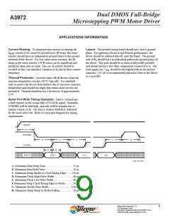
Dual DMOS Full-Bridge
Microstepping PWM Motor Driver
A3972
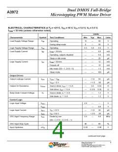
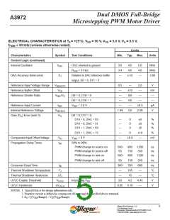
ELECTRICAL CHARACTERISTICS at TA = +25°C, VBB = 50 V, VDD = 5.0 V, VS = 0.5 V,
fPWM < 50 kHz (unless otherwise noted).
Limits
Characteristics
Symbol
fOSC
Test Conditions
Min.
Typ. Max.
Units
Control Logic (continued)
Internal Oscillator
OSC shorted to ground
ROSC = 51 k
3.0
3.4
—
4.0
4.0
5.0
4.6
—
MHz
MHz
LSB
DAC Accuracy (total error)
ET
Relative to DAC reference buffer
output, D0 = 0, D17 = 0
±1/2
Reference Input Voltage Range
Reference Buffer Offset
VREF(EXT)
VOS
0.5
—
—
±10
8.0
4.0
—
2.6
—
V
mV
—
—
μA
V
Reference Divider Ratio
VREF/VS
D0 = 0, D18 = 0
D0 = 0, D18 = 1
VREF = 2.0 V
—
—
—
—
Reference Input Current
Internal Reference Voltage
Gain (Gm) Error (note 3)
IREF
VREF(INT)
EG
—
±0.5
2.06
1.94
2.0
D0 = 0, D17 = 0,
D18 = 0, DAC = 63
D18 = 0, DAC = 31
D18 = 1, DAC = 63
—
—
—
0
0
0
±6
±9
±6
%
%
%
D18 = 1, DAC = 15
VREF = 0 V
—
—
0
±10
—
%
ComparatorInputOffsetVoltage
Propagation Delay Times
VIO
tpd
±5.0
mV
50% to 90%:
PWM change to source on
PWM change to source off
PWM change to sink on
500
50
800
150
800
1200
350
ns
ns
ns
500
1200
PWM change to sink off
50
300
—
150
700
165
15
350
900
—
ns
ns
°C
°C
V
Crossover Dead Time
tdt
TJ
Thermal Shutdown Temperature
Thermal Shutdown Hysteresis
UVLO Enable Threshold
UVLO Hysteresis
TJ
—
—
VUVLO
VUVLO
Increasing VDD
3.9
0.05
4.2
4.45
—
0.10
V
NOTES: 1. Typical Data is for design information only.
2. Negative current is defined as coming out of (sourcing) the specified device terminal.
3. EG = [(VREF/Range) – VS]/(VREF/Range).
Allegro MicroSystems, LLC
115 Northeast Cutoff
5
Worcester, Massachusetts 01615-0036 U.S.A.
1.508.853.5000; www.allegromicro.com

 ALLEGRO [ ALLEGRO MICROSYSTEMS ]