3946
Half-Bridge Power MOSFET Controller
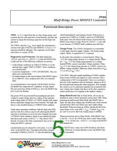
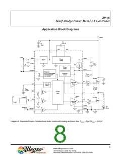
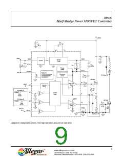
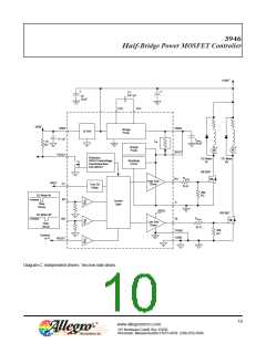
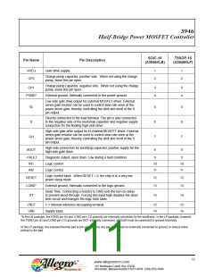
Application Information
At power-up and when the drivers have been disabled for
a long time, the bootstrap capacitor can be completely
discharged. In this case, Delta_v can be considered to be the
full high-side drive voltage, 12 V. Otherwise, Delta_v is the
Bootstrap Capacitor Selection. CBOOT must be cor-
rectly selected to ensure proper operation of the device. If
too large, time is wasted charging the capacitor, with the
result being a limit on the maximum duty cycle and PWM
frequency. If the capacitor is too small, the voltage drop can
be too large at the time the charge is transferred from the
CBOOT to the MOSFET gate.
amount of voltage dropped during the charge transfer, which
should be 400 mV or less. The capacitor is charged whenever
the S pin is pulled low, via a GL PWM cycle, and current
flows from VREG through the internal bootstrap diode
To keep the voltage drop small:
QBOOT >> QGATE
circuit to CBOOT
.
Power Dissipation. For high ambient temperature
applications, there may be little margin for on-chip power
consumption. Careful attention should be paid to ensure that
the operating conditions allow the A3946 to remain in a safe
range of junction temperature.
where a factor in the range of 10 to 20 is reasonable. Using
20 as the factor:
QBOOT = CBOOT
VBOOT = QGATE 20
×
×
and
CBOOT = QGATE 20 / V
×
BOOT
The power consumed by the A3946 can be estimated as:
P_total = Pd_bias + Pd_cpump + Pd_switching_loss
where:
The voltage drop on the BOOT pin, as the MOSFET is being
turned on, can be approximated by:
Delta_v = QGATE / CBOOT
Pd_bias = VBB
IVBB , typically 3 mA,
×
For example, given a gate charge, QGATE, of 160 nC, and the
typical BOOT pin voltage of 12 V, the value of the Boot
capacitor, CBOOT, can be determined by:
and
Pd_cpump = (2VBB – VREG) IAVE, for VBB < 15 V, or
Pd_cpump = (VBB – VREG) IAVE, for VBB > 15 V,
CBOOT = (160 nC 20) / 12 V ≈ 0.266 μF
×
Therefore, a 0.22 μF ceramic (X7R) capacitor can be chosen
for the Boot capacitor.
in either case, where
In that case, the voltage drop on the BOOT pin, when the
high-side MOSFET is turned on, is:
IAVE = Q
2
f
PWM
GATE × ×
and
Pd_switching_loss = QGATE
V
2
fPWM Ratio,
×
REG × ×
Delta_v = 160 nC / 0.22 μF = 0.73 V
where
Bootstrap Charging. It is good practice to ensure that the
high-side bootstrap capacitor is completely charged before a
high-side PWM cycle is requested.
Ratio = 10 ꢀ / (RGATE + 10 ꢀ).
The time required to charge the capacitor can be approxi-
mated by:
tCHARGE = CBOOT (Delta_v / 100 mA)
7
www.allegromicro.com
115 Northeast Cutoff, Box 15036
Worcester, Massachusetts 01615-0036 (508) 853-5000

 ALLEGRO [ ALLEGRO MICROSYSTEMS ]