3946
Half-Bridge Power MOSFET Controller
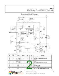
The dead time circuit can be disabled by tying the DT pin
to VREF. This disables the turn-on delay and allows direct
control of each MOSFET gate via two control lines. This is
shown in the Control Logic table, on page 2.
Dead Time. The analog input pin DT sets the delay to turn
on the high- or low-side gate outputs. When instructed to
turn off, the gate outputs change after an short internal propa-
gation delay (90 ns typical). The dead time controls the time
between this turn-off and the turn-on of the appropriate gate.
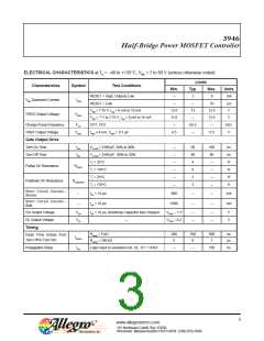
The duration, tDEAD, can be adjusted within the range 350 ns
to 6000 ns using the following formula:
Top-Off Charge Pump. An internal charge pump allows
100% duty cycle operation of the high-side MOSFET. This is
a low-current trickle charge pump, and is only operated after
a high-side has been signaled to turn on. A small amount
of bias current (< 200 μA) is drawn from the BOOT pin
to operate the floating high-side circuit. The charge pump
simply provides enough drive to ensure that the gate voltage
does not droop due to this bias supply current. The charge
required for initial turn-on of the high-side gate must be sup-
plied by bootstrap capacitor charge cycles. This is described
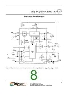
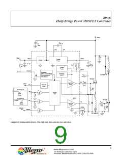
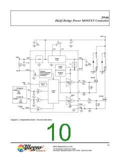
in the section Application Information.
tDEAD = 50 + (RDEAD ⁄ 16.7)
where tDEAD is in ns, and RDEAD is in Ω, and should be in the
range 5 kΩ < RDEAD < 100 kΩ.
Do not ground the DT pin. If the DT pin is left open, dead
time defaults to 12 μs.
Control Logic. Two different methods of control are
possible with the A3946. When a resistor is connected from
DT to ground, a single-pin PWM scheme is utilized by short-
ing IN1 with IN2. If a very slow turn-on is required (greater
than 6 μs), the two input pins can be hooked-up individually
to allow the dead times to be as long as needed.
VREF. VREF is used for the internal logic circuitry and
is not intended as an external power supply. However,
the VREF pin can source up to 4 mA of current. A 0.1 μF
capacitor is needed for decoupling.
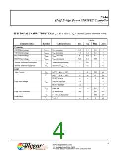
Fault Response Table
Fault Mode
RESET
~FAULT
VREG
ON
VREF
ON
GH1
(IL)
0
GL1
(IL)
(IL)
0
No Fault
1
1
1
1
1
0
1
0
0
0
0
1
BOOT Capacitor Undervoltage2
VREG Undervoltage3
VREF Undervoltage4
Thermal Shutdown3
Sleep5
ON
ON
ON
ON
0
OFF
ON
ON
0
0
ON
(IL)
High Z
(IL)
High Z
OFF
OFF
1(IL) indicates that the state is determined by the input logic.
2This fault occurs whenever there is an undervoltage on the BOOT capacitor. This fault is not latched.
3These faults are latched. Clear by pulsing RESET = 0.
4Unspecified VREF undervoltage threshold < 4 V.
5During power supply undervoltage conditions, GH and GL are instructed to be 0 (low). However, with VREG < 4 V, the outputs start to be-
come high impedance (High Z). Refer to the section Sleep Mode/Power Up.
6
www.allegromicro.com
115 Northeast Cutoff, Box 15036
Worcester, Massachusetts 01615-0036 (508) 853-5000

 ALLEGRO [ ALLEGRO MICROSYSTEMS ]