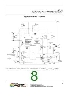
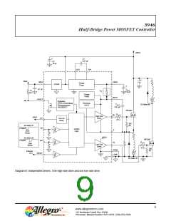
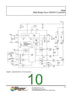
3946
Half-Bridge Power MOSFET Controller
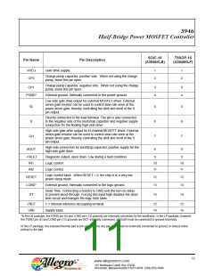
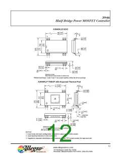
SOIC-16
(A3946KLB)
TSSOP-16
(A3946KLP)
Pin Name
Pin Description
VREG
CP2
Gate drive supply.
1
2
1
2
Charge pump capacitor, positive side. When not using the charge
pump, leave this pin open.
Charge pump capacitor, negative side. When not using the charge
pump, leave this pin open.
CP1
3
4
3
4
PGND*
External ground. Internally connected to the power ground.
Low-side gate drive output for external MOSFET driver. External
series gate resistor can be used to control slew rate seen at the
power driver gate, thereby controlling the di/dt and dv/dt of the S
pin output.
GL
S
5
6
5
6
Directly connected to the load terminal. The pin is also connected
to the negative side of the bootstrap capacitor and negative supply
connection for the floating high-side drive.
High-side gate drive output for N-channel MOSFET driver. External
series gate resistor can be used to control slew rate seen at the
power driver gate, thereby controlling the di/dt and dv/dt of the S
pin output.
GH
7
8
7
8
High-side connection for bootstrap capacitor, positive supply for the
high-side gate drive.
BOOT
~FAULT
IN1
Diagnostic output, open drain. Low during a fault condition.
9
9
Logic control.
Logic control.
10
11
10
11
IN2
Logic control input. When RESET = 0, the chip is in a very low
power sleep mode.
RESET
LGND*
12
13
12
13
External ground. Internally connected to the logic ground.
Dead Time. Connecting a resistor to GND sets the turn-on delay
to prevent shoot-through. Forcing this input high disables the dead
time circuit and changes the logic truth table.
DT
14
14
VREF
VBB
5 V internal reference decoupling terminal.
Supply Input.
15
16
15
16
*In the LB package, the PGND pin (4) and LGND pin (13) grounds are internally connected by the leadframe. In the LP package, however,
the PGND pin (4) and LGND pin (13) grounds are NOT internally connected, and both must be connected to ground externally.
In the LP package, the exposed thermal pad is not connected to any pin, but should be externally connected to ground, to reduce noise
pickup by the pad.
11
www.allegromicro.com
115 Northeast Cutoff, Box 15036
Worcester, Massachusetts 01615-0036 (508) 853-5000

 ALLEGRO [ ALLEGRO MICROSYSTEMS ]