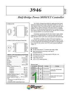
3946
Half-Bridge Power MOSFET Controller
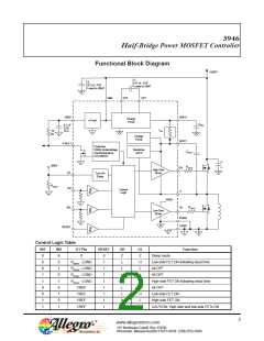
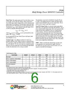
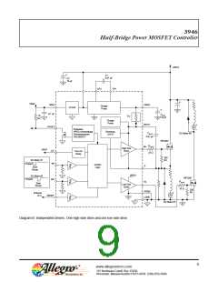
Functional Description
cleared immediately, and remains cleared. If the power is
restored (no UVREG or UVREF), and if no OVERTEMP
fault exists, then the latched fault remains cleared when the
RESET line returns to high. However, FAULT = 1 may still
occur because a UVBOOT fault condition may still exist.
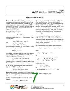
VREG. A 13 V output from the on-chip charge pump, used
to power the low-side gate drive circuit directly, provides the
current to charge the bootstrap capacitors for the high-side
gate drive.
The VREG capacitor, CREG, must supply the instantaneous
current to the gate of the low-side MOSFET. A 10 μF, 25 V
capacitor should be adequate. This capacitor can be either
electrolytic or ceramic (X7R).
Charge Pump. The A3946 is designed to accommodate
a wide range of power supply voltages. The charge pump
output, VREG, is regulated to 13 V nominal.
Diagnostics and Protection. The fault output pin,
~FAULT, goes low (i.e., FAULT = 1) when the RESET line
is high and any of the following conditions are present:
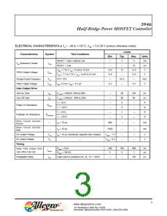
In all modes, this regulator is current-limited. When VBB
< 8 V, the charge pump operates as a voltage doubler. When
8V < VBB< 15V, the charge pump operates as a voltage
doubler/PWM, current-controlled, voltage regulator. When
VBB>15V, the charge pump operates as a PWM, current-con-
trolled, voltage regulator. Efficiency shifts, from 80% at VBB=
7 V, to 20% at VBB = 50 V.
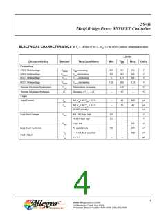
• Undervoltage conditions on VREG (UVREG) or on the
internal logic supply VREF (UVREF). These conditions
set a latched fault.
• A junction temperature > 170°C (OVERTEMP). This con-
dition sets a latched fault.
CAUTION. Although simple paralleling of VREG supplies
from several A3946s may appear to work correctly, such a
configuration is NOT recommended. There is no assurance
that one of the regulators will not dominate, taking on all of
the load and back-biasing the other regulators. (For example,
this could occur if a particular regulator has an internal refer-
ence voltage that is higher that those of the other regulators,
which would force it to regulate at the highest voltage.)
• An undervoltage on the stored charge of the BOOT capaci-
tor (UVBOOT). This condition does NOT set a latched
fault.
An overtemperature event signals a latched fault, but does
not disable any output drivers, regulators, or logic inputs.
The user must turn off the A3946 (e.g., force the RESET line
low) to prevent damage.
Sleep Mode/Power Up. In Sleep Mode, all circuits are
disabled in order to draw minimum current from VBB. When
powering up and leaving Sleep Mode (the RESET line is
high), the gate drive outputs stay disabled and a fault remains
asserted until VREF and VREG pass their undervoltage
thresholds. When powering up, before starting the first boot-
strap charge cycle, wait until t = CREG ⁄ 4 (where CREG is in
μF, and t is in ns) to allow the charge pump to stabilize.
The power FETs are protected from inadequate gate drive
voltage by undervoltage detectors. Either of the regulator
undervoltage faults (UVREG or UVREF) disable both output
drivers until both voltages have been restored. The high-side
driver is also disabled during a UVBOOT fault condition.
Under many operating conditions, both the high-side (GH)
and low-side (GL) drivers may be off, allowing the BOOT
capacitor to discharge (or never become charged) and create
a UVBOOT fault condition, which in turn inhibits the high-
side driver and creates a FAULT = 1. This fault is NOT
latched. To remove this fault, momentarily turn on GL to
charge the BOOT capacitor.
When powered-up (not in Sleep Mode), if the RESET line
is low for > 10 μs, the A3946 may start to enter Sleep Mode
(VREF < 4 V). In that case, ~FAULT = 1 as long as the RESET
line remains low.
If the RESET line is open, the A3946 should go into Sleep
Mode. However, to ensure that this occurs, the RESET line
must be grounded.
Latched faults may be cleared by a low pulse, 1 to 10 μs
wide, on the RESET line. Throughout that pulse (despite
a possible UVBOOT), FAULT = 0; also the fault latch is
5
www.allegromicro.com
115 Northeast Cutoff, Box 15036
Worcester, Massachusetts 01615-0036 (508) 853-5000

 ALLEGRO [ ALLEGRO MICROSYSTEMS ]