[AK4679]
■ Command Code map for the DSP
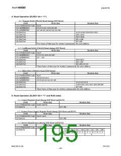
1. Command Code
BIT7
BIT6
BIT5
BIT4
BIT3
BIT2
BIT1
BIT0
R/W flag
Area to be accessed
Accompanying data to the access area
R/W Flag
Write at “1”, Read at “0”.
Access data and accompanying data
BIT6
BIT5
BIT4 BIT3~0
0
0
0
0
0
1
0
1
0
Number of Write
Number of Write
0100
0010
1000
0100
0010
Register Address
Register Address
0000
Write preparation to CRAM during RUN
Write preparation to OFREG during RUN
Write operation to CRAM during RUN
Write operation to OFREG during RUN
Write operation to PRAM during DSP reset
Write operation to CRAM during DSP reset
Write operation to OFREG during DSP reset
Internal control registers 00h~08h
System power registers 00h~01h
Device Identification (Read only)
Error Status Read
0
1
1
1
1
1
1
0
0
1
1
0
1
0
1
0000
0010
CRC Write/Read
0100
Write operation of JX code
0110
Read operation from MIR1
1000
Read operation from MIR2
1010
Read operation from MIR3
1100
Read operation from MIR4
2. Address
Address description is always LSB justified. Accessing command code BIT[6:4]= “000” to “011” requires 16bit address.
Accessing command code BIT[6:4]= “100” to “111” requires no address.
3. Data
Length of write data is depending on the writing area size. When accessing RAM, data may be written to sequential
address locations by writing data continuously.
MS1402-E-06
2013/02
- 191 -

 AKM [ ASAHI KASEI MICROSYSTEMS ]