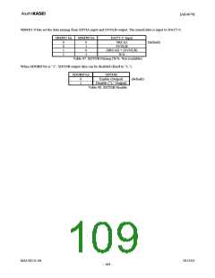
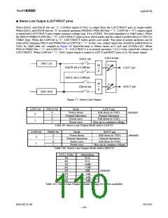
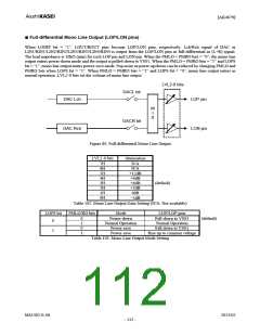
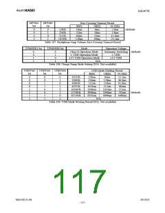
[AK4679]
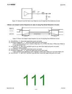
<Full-differential Mono Line Output Control Sequence (in case of using Pop Noise Reduction
Circuit)>
(2 )
(5 )
P M L O b it
P M R O b it
(1)
(3 )
(4 )
(6 )
L O P S bit
L O P , L O N p in s
N o rm a l O utp u t
≥ 3 0 0 m s
≥ 3 0 0 m s
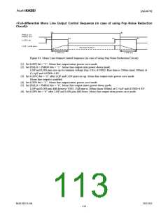
Figure 81. Mono Line Output Control Sequence (in case of using Pop Noise Reduction Circuit)
(1) Set LOPS bit = “1”. Mono line output enters power-save mode.
(2) Set PMLO = PMRO bits = “1”. Mono line output exits power-down mode.
LOP and LON pins rise up to common voltage (typ. 0.8 x AVDD). Rise time is 200ms (max 300ms) at
C=1μF and AVDD=1.8V.
(3) Set LOPS3 bit = “0” after LOP and LON pins rise up. Mono line output exits power-save mode.
Mono line output is enabled.
(4) Set LOPS bit = “1”. Mono line output enters power-save mode.
(5) Set PMLO = PMRO bits = “0”. Mono line output enters power-down mode.
LOP and LON pins fall down to VSS1. Fall time is 200ms (max 300ms) at C=1μF and AVDD=1.8V.
(6) Set LOPS bit = “0” after LOP and LON pins fall down. Mono line output exits power-save mode.
MS1402-E-06
2013/02
- 113 -

 AKM [ ASAHI KASEI MICROSYSTEMS ]