[AK4646]
■ Stereo Line Output
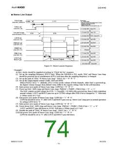
Example:
FS3-0 bits
0,000
1,111
91H
PLL, Master Mode
(Addr:05H, D5&D2-0)
Audio I/F Format :MSB justified (ADC & DAC)
Sampling Frequency:44.1KHz
Digital Volume: 0dB
(1)
(9)
MGAIN1=SPKG1=SPKG0=BEEPL bits = “0”
DACL bit
(Addr:02H, D4)
(2)
(1) Addr:05H, Data:27H
(2) Addr:02H, Data:10H
(3) Addr:0AH&0DH, Data:91H
(4) Addr:03H, Data:40H
(5) Addr:00H, Data:6CH
(6) Addr:03H, Data:00H
Playback
OVL/R7-0 bits
(Addr:0AH&0DH, D7-0)
91H
(3)
LOPS bit
(Addr:03H, D6)
(4)
(6)
(7)
(10)
PMDAC bit
(Addr:00H, D2)
PMBP bit
(Addr:00H, D5)
(5)
(8)
(7) Addr:03H, Data:40H
(8) Addr:00H, Data:40H
(9) Addr:02H, Data:00H
(10) Addr:03H, Data:00H
PMLO bit
(Addr:00H, D3)
>300 ms
>300 ms
LOUT pin
ROUT pin
Normal Output
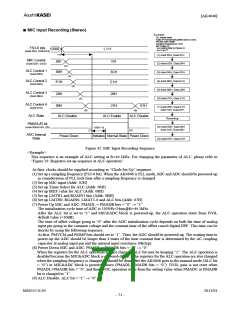
Figure 45. Stereo Lineout Sequence
<Example>
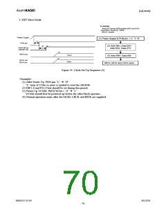
At first, clocks should be supplied according to “Clock Set Up” sequence.
(1) Set up the sampling frequency (FS3-0 bits). When the AK4646 is PLL mode, DAC and Stereo Line-Amp
should be powered-up in consideration of PLL lock time after the sampling frequency is changed.
(2) Set up the path of “DAC Æ Stereo Line Amp”: DACL bit = “0” Æ “1”
(3) Set up the output digital volume (Addr: 0AH and 0DH)
When OVOLC bit is “1” (default), OVL7-0 bits set the volume of both channels. After DAC is powered-up,
the digital volume changes from default value (0dB) to the register setting value by the soft transition.
(4) Enter power-save mode of Stereo Line Amp: LOPS bit = “0” Æ “1”
(5) Power-up DAC, MIN-Amp and Stereo Line-Amp: PMDAC = PMBP = PMLO bits = “0” → “1”
The DAC outputs invalid voltage for 67/fs = 1.52ms@fs = 44.1kHz after powered-up, then it starts outputting
normal voltage. LOUT and ROUT pins rise up to VCOM voltage after PMLO bit is changed to “1”. Rise time
is 300ms (max) at C=1μF.
(6) Exit power-save mode of Stereo Line-Amp: LOPS bit = “1” Æ “0”
LOPS bit should be set to “0” after LOUT and ROUT pins rise up. Stereo Line-Amp goes to normal operation
by setting LOPS bit to “0”.
(7) Enter power-save mode of Stereo Line-Amp: LOPS bit: “0” Æ “1”
(8) Power-down DAC, MIN-Amp and Stereo Line-Amp: PMDAC = PMBP = PMLO bits = “1” → “0”
LOUT and ROUT pins fall down to AVSS. Fall time is 300ms (max) at C=1μF.
(9) Disable the path of “DAC Æ Stereo Line-Amp”: DACL bit = “1” Æ “0”
(10)Exit power-save mode of Stereo Line-Amp: LOPS bit = “1” Æ “0”
LOPS bit should be set to “0” after LOUT and ROUT pins fall down.
MS0557-E-05
2011/01
- 74 -

 AKM [ ASAHI KASEI MICROSYSTEMS ]