ASAHI KASEI
[AK4115]
3. Validity bit
3-1. RX
In synchronous mode, the validity bit is available on the VOUT pin according to block start timing. In asynchronous
mode, the validity bit is available on the VOUT pin according to LRCK timing. The VRX bit is available in both modes.
The validity bit is outputted from SDTO pin with audio data in AES3 mode.
3-2. TX
The validity bit is controlled by the VIN pin or the VTX bit. Since the validity bit does not usually update every
sub-frame cycle, it can be controlled by the VIN pin according to LRCK timing in synchronous mode. In asynchronous
mode, it can be controlled by the VIN pin according to ELRCK timing. When the validity bit timing is synchronized with
the block start timing , the BCU_IO bit should be “0”. In asynchronous mode, the validity bit cannot be controlled by the
VIN pin when BCU_IO bit is set to “0”.
The input to VIN pin and VTX bit are ignored in AES3 mode and the validity bit on DAUX is outputted with audio data
from TX.
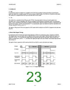
4. Block Start Signal Timing
In synchronous mode, the block start signal timing depends on LRCK. In asynchronous mode, it depends on ELRCK.
The channel status, user and validity bits are captured with the current audio sample. When the block start signal is an
input (BCU_IO bit = “0”), the block start signal should stay high for more than one sub-frame. When the block start
signal is an output (BCU_IO bit = “1”), the block start signal goes high at the start of frame 0 and remains high until the
end of frame 39.
The input to B pin is ignored in AES3 mode and the B bit on DAUX is used as the block start timing.
B (Input)
Don’t care
Don’t care
B (Output)
C (or U,V)
C(R191)
C(L0)
C(R0) C(L1)
C(L38) C(R39) C(L40)
LRCK(ELRCK)
(Except I2S)
LRCK(ELRCK)
(I2S)
SDTO (DAUX)
R191
L0
R0
L1
L38
R39
L40
Figure 17. B, C, U, V Input/output timings
MS0573-E-00
2006/12
- 23 -

 AKM [ ASAHI KASEI MICROSYSTEMS ]