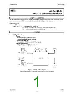
ASAHI KASEI
[AKD4113-B]
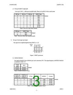
(2) Evaluation for DIT
S/PDIF in (optical or BNC)– AK4113 – S/PDIF out (optical or BNC)
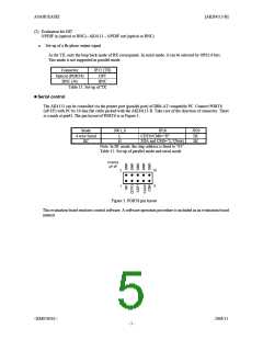
a. Set-up of a Bi-phase output signal
As for TX, only the loop back mode of RX corresponds. In serial mode, it can be selected by OPS2-0 bits.
This mode is not supported in parallel mode.
Connector
Optical (PORT4)
BNC (J4)
JP13 (TX)
OPT
BNC
Table 11. Set-up of TX
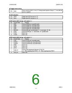
Serial control
The AK4113 can be controlled via the printer port (parallel port) of IBM-AT compatible PC. Connect PORT6
(uP-I/F) with PC by 10-line flat cable packed with the AKD4113-B. Take care of the direction of connector. There
is a mark at pin#1. The pin layout of PORT6 is as Figure 3.
Mode
4 wire Serial
IIC
SW1_6
JP18
CDTO/CM0=“H”
SDA and CM0=“L”(Note)
JP20
IIC
IIC
L
H
Note: In IIC mode, the chip address is fixed to “01”.
Table 12. Set-up of parallel mode and serial mode
PORT6
uP I/F
2
1
10
9
Figure 3. PORT6 pin layout
This evaluation board encloses control software. A software operation procedure is included in an evaluation board
manual.
<KM076501>
2004/11
- 5 -

 AKM [ ASAHI KASEI MICROSYSTEMS ]