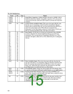
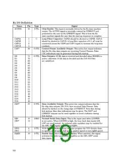
Tx I/O Definition
Name
Pin
Type
Signal
CAP0A
2
1
3
4
C
Loop Filter Capacitor: CAP0A should be shorted to CAP0B. CAP1A
should be shorted to CAP1B. A loop filter capacitor of 0.1 µf must be
connected across the CAP0 and CAP1 inputs to increase the loop time
constant.
CAP0B
CAP1A
CAP1B
CAV*
69
I-TTL Control Word Available Input: This active-low input tells the chip
that the user is requesting a control word be transmitted. This pin
should only be asserted after the user has determined the RFD line is
active for a given frame cycle. When this pin is asserted, the
information on the Data inputs is sent as a control frame. If CAV and
DAV are asserted simultaneously, CAV takes precedence.
D0
D1
D2
D3
D4
D5
D6
D7
59
58
57
56
55
54
53
51
50
49
48
47
46
45
40
39
38
37
36
35
I-TTL Data Inputs: 20 Bit data is encoded and transmitted when M20SEL
is active; otherwise the 16 least significant bits are encoded and
transmitted. The encoded bits are transmitted LSB first (e.g.: D0 is
sent first, through to either D15 or D19, followed by the 4 coding bits
C0-C3).
D8
D9
D10
D11
D12
D13
D14
D15
D16
D17
D18
D19
DAV*
70
I-TTL Data Available Input: This active-low input tells the chip that the
user has valid data to be transmitted. This pin should be asserted only
after the user has determined that the RFD line is active for a given
frame cycle. When this pin is asserted, the information on the Data
and Flag inputs is encoded and sent as a Data frame.
DIV0
DIV1
19
20
I-TTL VCO Divider Select: These two pins program the VCO divider chain
to operate at full speed, half speed, quarter speed, or one-eighth speed.
DOUT
DOUT*
17
18
O-BLL Normal Serial Data Output: Output used when LOOPEN is not
active. This output is a special buffer line logic driver, which is a 50 Ω
back-terminated ECL compatible output.
ED
67
I-TTL Enable Data: This signal comes from the Rx chip state machine and
is used to control the RFD output of the Tx chip. The state machine
only allows data to be enabled when both sides of the link have
established stable lock.
630

 AGILENT [ AGILENT TECHNOLOGIES, LTD. ]