5
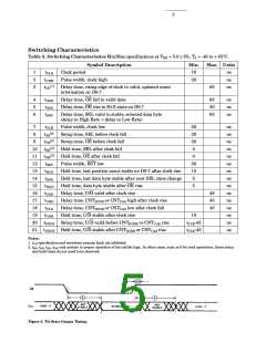
Switching Characteristics
Table 5. Switching Characteristics Min/Max specifications at VDD = 5.0 ± 5%, TA = -40 to + 85°C.
Symbol Description
Min.
70
Max. Units
1
2
3
tCLK
tCHH
Clock period
ns
ns
Pulse width, clock high
28
[1]
tCD
Delay time, rising edge of clock to valid, updated count
information on D0-7
65
ns
4
5
6
tODE
tODZ
tSDV
Delay time, OE fall to valid data
65
40
65
ns
ns
ns
Delay time, OE rise to Hi-Z state on D0-7
Delay time, SEL valid to stable, selected data byte
(delay to High Byte = delay to Low Byte)
7
tCLH
Pulse width, clock low
28
20
20
0
ns
ns
ns
ns
ns
ns
ns
ns
ns
ns
ns
ns
ns
ns
ns
[2]
8
tSS
Setup time, SEL before clock fall
[2]
9
tOS
Setup time, OE before clock fall
[2]
10
11
12
13
14
15
16
17
18
19
20
tSH
Hold time, SEL after clock fall
[2]
tOH
Hold time, OE after clock fall
0
tRST
tDCD
tDSD
tDOD
tUDD
tCHD
tCLD
tUDH
Pulse width, RST low
28
10
5
Hold time, last position count stable on D0-7 after clock rise
Hold time, last data byte stable after next SEL state change
Hold time, data byte stable after OE rise
Delay time, U/D valid after clock rise
Delay time, CNTDCDR or CNTCAS high after clock rise
Delay time, CNTDCDR or CNTCAS low after clock fall
Hold time, U/D stable after clock rise
5
45
45
45
10
tUDCS Setup time, U/D valid before CNTDCDR or CNTCAS rise
tCLK-45
tCLK-45
21 tUDCH Hold time, U/D stable after CNTDCDR or CNTCAS rise
Notes:
1. tCD specification and waveform assume latch not inhibited.
2. tSS, tOS, tSH, tOH only pertain to proper operation of the inhibit logic. In other cases, such as 8 bit read operations, these setup
and hold times do not need to be observed.
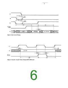
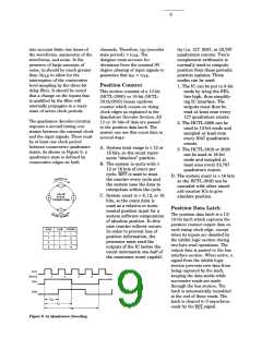
Figure 3. Tri-State Output Timing.

 AGILENT [ AGILENT TECHNOLOGIES, LTD. ]