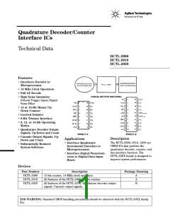
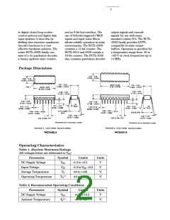
3
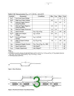
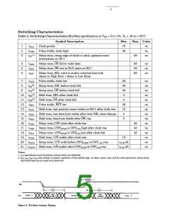
Table 3. DC Characteristics VDD = 5 V ± 5%; TA = -40 to 85°C
Symbol
Parameter
Condition
Min. Typ. Max. Unit
[2]
V
Low-Level Input Voltage
High-Level Input Voltage
1.5
V
V
V
IL
[2]
VIH
3.5
VT+
VT-
Schmitt-Trigger Positive-
Going Threshold
3.5
1.5
4.0
Schmitt-Trigger Negative-
Going Threshold
1.0
V
VH
IIN
Schmitt-Trigger Hysteresis
Input Current
1.0
-10
2.4
2.0
1
V
µA
V
VIN = VSS or VDD
+10
[2]
VOH
High-Level Output
Voltage
IOH -1.6 mA
4.5
[2]
VOL
Low-Level Output
Voltage
IOL = +4.8 mA
VO = VSS or VDD
0.2
1
0.4
+10
5
V
IOZ
High-Z Output Leakage
Current
-10
µA
IDD
CIN
Quiescent Supply Current
Input Capacitance
VIN = VSS or VDD, VO = HiZ
Any Input[3]
Any Output[3]
1
5
6
µA
pF
pF
COUT
Output Capacitance
Notes:
1. Free air.
2. In general, for any VDD between the allowable limits (+4.5 V to +5.5 V), VIL = 0.3 VDD and VIH = 0.7 VDD; typical values are
VOH = VDD - 0.5 V @ IOH = -40 µA and VOL = VSS + 0.2 V @ IOL = 1.6 mA.
3. Including package capacitance.
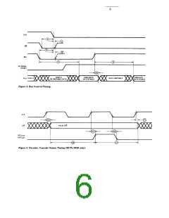
Figure 1. Reset Waveform.
Figure 2. Waveform for Positive Clock Related Delays.

 AGILENT [ AGILENT TECHNOLOGIES, LTD. ]