10
Inhibit Logic
output and whether or not the
output bus is in the high-Z state.
In the case of the HCTL-2000 the
data latch is only 12 bits wide
and the upper four bits of the
high byte are internally set to
zero.
will be set to the proper voltage
level one clock cycle before the
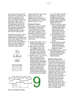
The Inhibit Logic Section samples
the OE and SEL signals on the
falling edge of the clock and, in
response to certain conditions
(see Figure 10 below), inhibits
the position data latch. The RST
signal asynchronously clears the
inhibit logic, enabling the latch. A
simplified logic diagram of the
inhibit circuitry is illustrated in
Figure 11.
rising edge of the CNT
DCDR
pulse, and held one clock cycle
after the rising edge of the
CNT
pulse. These outputs
DCDR
are not affected by the inhibit
logic. See Figures 5 and 12 for
detailed timing.
Quadrature Decoder
Output (HCTL-2020
Only)
The quadrature decoder output
section consists of count and up/
down outputs derived from the
4X decode logic of the HCTL-
2020. When the decoder has
detected a count, a pulse, one-
half clock cycle long, will be
Cascade Output (HCTL-
2020 Only)
The cascade output also consists
of count and up/down outputs.
When the HCTL-2020 internal
counter overflows or underflows,
a pulse, one-half clock cycle long,
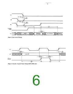
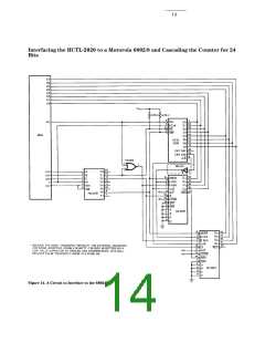
Bus Interface
The bus interface section consists
of a 16 to 8 line multiplexer and
an 8-bit, three-state output
buffer. The multiplexer allows
independent access to the low
and high bytes of the position
data latch. The SEL and OE
signals determine which byte is
will be output on the CNT
pin.
CAS
output on the CNT
pin. This
This output will occur during the
clock cycle in which the internal
counter is updated. The U/D pin
will be set to the proper voltage
level one clock cycle before the
DCDR
output will occur during the clock
cycle in which the internal
counter is updated. The U/D pin
rising edge of the CNT
pulse,
CAS
Inhibit
Step SEL OE CLK Signal
and held one clock cycle after the
rising edge of the CNT pulse.
Action
CAS
These outputs are not affected by
the inhibit logic. See Figures 5
and 12 for detailed timing.
1
2
3
L
H
X
L
L
1
1
0
Set inhibit; read high byte
Read low byte; starts reset
Completes inhibit logic reset
H
Figure 10. Two Byte Read Sequence.
Figure 11. Simplified Inhibit Logic.

 AGILENT [ AGILENT TECHNOLOGIES, LTD. ]