AD9834
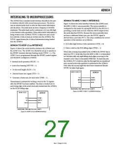
AD9834 TO 80C51/80L51 INTERFACE
AD9834 TO DSP56002 INTERFACE
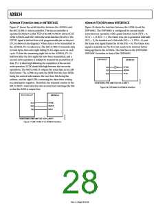
Figure 37 shows the serial interface between the AD9834 and
the 80C51/80L51 microcontroller. The microcontroller is
operated in Mode 0 so that TXD of the 80C51/80L51 drives SCLK
of the AD9834, and RXD drives the serial data line (SDATA). The
FSYNC signal is derived from a bit programmable pin on the port
(P3.3 is shown in the diagram). When data is to be transmitted to
the AD9834, P3.3 is taken low. The 80C51/80L51 transmits data
in 8-bit bytes, thus only eight falling SCLK edges occur in each
cycle. To load the remaining eight bits to the AD9834, P3.3 is
held low after the first eight bits have been transmitted, and a
second write operation is initiated to transmit the second byte of
data. P3.3 is taken high following the completion of the second
write operation. SCLK should idle high between the two write
operations. The 80C51/80L51 outputs the serial data in an LSB-
first format. The AD9834 accepts the MSB first (the four MSBs
being the control information, the next four bits being the
address, and the eight LSBs containing the data when writing
to a destination register). Therefore, the transmit routine of the
80C51/80L51 must take this into account and rearrange the bits
so that the MSB is output first.
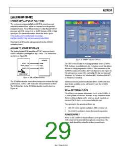
Figure 38 shows the interface between the AD9834 and the
DSP56002. The DSP56002 is configured for normal mode
asynchronous operation with a gated internal clock (SYN = 0,
GCK = 1, SCKD = 1). The frame sync pin is generated internally
(SC2 = 1), the transfers are 16 bits wide (WL1 = 1, WL0 = 0), and
the frame sync signal frames the 16 bits (FSL = 0). The frame sync
signal is available on Pin SC2, but needs to be inverted before
being applied to the AD9834. The interface to the DSP56000/
DSP56001 is similar to that of the DSP56002.
DSP560021
AD98341
FSYNC
SDATA
SC2
STD
SCK
SCLK
1
ADDITIONAL PINS OMITTED FOR CLARITY.
Figure 38. DSP56002 to AD9834 Interface
80C51/80L511
AD98341
FSYNC
SDATA
P3.3
RXD
TXD
SCLK
1
ADDITIONAL PINS OMITTED FOR CLARITY.
Figure 37. 80C51/80L51 to AD9834 Interface
Rev. C | Page 28 of 36

 ADI [ ADI ]