AD5940
Data Sheet
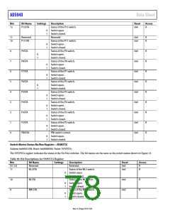
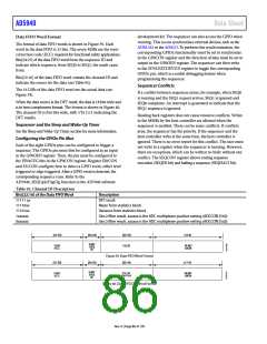
Bits
Bit Name
Settings Description
ADC 1.11 V low power common-mode buffer (optional). Use the high speed
Reset Access
5
V1P1LPADCEN
0x1
R/W
or low power reference buffer.
0
1
Disables the 1.11 V low power reference buffer of the ADC.
Enables the 1.11 V low power reference buffer of the ADC.
4
3
V1P1HSADCEN
Enables the 1.11 V, high speed, common-mode buffer. This bit controls the
buffer for the 1.11 V common-mode voltage source to the ADC input stage.
Disables the 1.11 V, high speed, common-mode buffer.
Enables the 1.11 V, high speed, common-mode buffer (recommended value
for normal ADC operation).
0x1
R/W
0
1
V1P8HSADCCHGDIS
V1P8LPADCEN
Controls the decoupling capacitor discharge switch. This switch connects
the 1.82 V internal ADC reference to an internal discharging circuit. Leave
this bit open for normal operation to maintain the reference voltage on the
external decoupling capacitor.
Opens switch. If opened, the voltage on the external decoupling capacitor
for the reference is maintained (recommended value).
0x0
0x1
R/W
R/W
0
1
Closes switch. Close this switch to connect the reference to the discharge circuit.
ADC 1.82 V low power reference buffer.
2
0
1
Disables the low power 1.82 V reference buffer.
Enables the low power 1.82 V reference buffer (recommended value). This
setting speeds up the settling time when exiting a power-down state.
1
0
V1P8HSADCILIMITEN
V1P8HSADCEN
High speed ADC input current limit. This bit protects the ADC input buffer.
Disables buffer current limit.
Enables buffer current limit (recommended value).
0x1
0x1
R/W
R/W
0
1
High speed 1.82 V reference buffer. Enable the reference buffer for normal
ADC conversions.
0
1
Disables 1.82 V high speed ADC reference buffer.
Enables 1.82 V high speed ADC reference buffer.
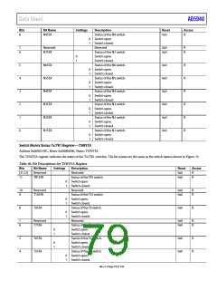
Rev. 0 | Page 82 of 130

 ADI [ ADI ]