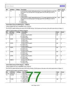
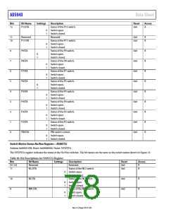
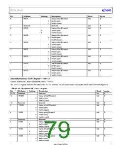
Data Sheet
AD5940
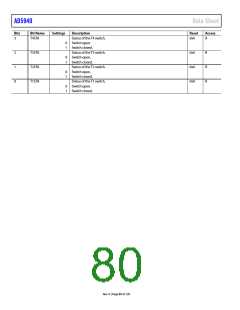
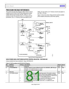
PRECISION VOLTAGE REFERENCES
This section describes the integrated voltage reference options
available on the AD5940. The AD5940 can generate accurate
voltage references for the ADC and DAC. There is a 1.82 V
reference for the ADC and DAC and a 2.5 V reference for the
potentiostat. The 2.5 V reference must be decoupled via the
VREF_2V5 pin and the 1.82 V reference must be decoupled via
the VREF_1V82 pin.
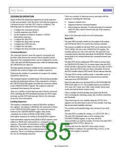
Figure 34 shows the various voltage reference options available
and the register and bits that control these options.
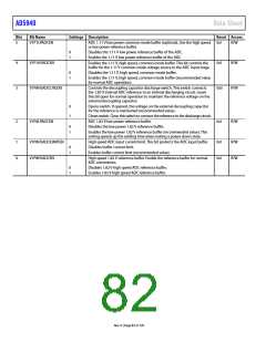
AVDD
AIN3/BUF_VREF1V8
1.82V FOR
THERMISTOR
1.82V
ANALOG
LDO
BUFSENCON[8]
VBIAS_CAP
4.7µF
1.1V FOR ADC
INPUT BIAS
1.82V AVDD
HP ADC
BUFSENCON[4]
BUFFER
1.1V HP
PRECISION
BAND GAP
VREF_1V82
4.7µF
1.82V
REFERENCE
FOR ADC
BUFSENCON[0]
AFECON[5]
HP DAC
BUFFER
1.82V
REFERENCE
FOR ADC
BUFSENCON[2]
ULP
BUFFER
0.92V
LP
BAND GAP
VREF_2V5
0.47µF
2.5V
REFERENCE
LP ADC
BUFFER
FOR POTENTIOSTAT
1.82V
REFERENCE
FOR ADC
LOW POWER 1.11V
BUFFER
BUFSENCON[2]
VOLTAGE REFERENCES
BUFSENCON[5]
Figure 34. Precision Voltage References
HIGH POWER AND LOW POWER BUFFER CONTROL REGISTER—BUFSENCON
Address 0x00002180, Reset: 0x00000037, Name: BUFSENCON
Table 91. Bit Descriptions for BUFSENCON Register
Bits
Bit Name
Settings Description
Reset Access
[31:9] Reserved
Reserved.
0x0
0x0
R
8
V1P8THERMSTEN
Buffered reference output. Buffered output to the AIN3/BUF_VREF1V82 pin.
R/W
0
1
Disables 1.82 V buffered reference output.
Enables 1.82 V buffered reference output.
Reserved.
7
6
Reserved
0x0
0x0
R
V1P1LPADCCHGDIS
Controls the decoupling capacitor discharge switch. This switch connects
the 1.11 V internal reference for the ADC common-mode voltage to an internal
discharging circuit. Leave this bit open for normal operation to maintain the
reference voltage on the external 1.11 V decoupling capacitor.
R/W
0
1
Opens switch (recommended value). Leave the switch open to maintain
charge on external decoupling capacitor for the 1.11 V reference.
Closes switch. Close this switch to connect the 1.11 V reference to the
discharging circuit.
Rev. 0 | Page 81 of 130

 ADI [ ADI ]