Data Sheet
AD5940
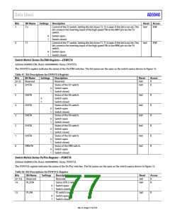
Bits
1
Bit Name
T2
Settings Description
Control of the T2 switch. Setting this bit closes T2. T2 is open if this bit is not set. This
Reset Access
0x0
R/W
bit connects the inverting input of the high speed TIA to the AIN1 pin via the T9
switch.
0
1
Switch open.
Switch closed.
0
T1
Control of the T1 switch. Setting this bit closes T1. T1 is open if this bit is not set. This
bit connects the inverting input of the high speed TIA to the AIN0 pin via the T9
switch.
0x0
R/W
0
1
Switch open.
Switch closed.
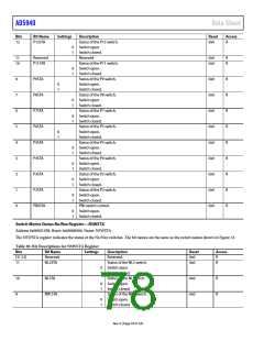
Switch Matrix Status Dx/DR0 Register—DSWSTA
Address 0x000021B0, Reset: 0x00000000, Name: DSWSTA
The DSWSTA register indicates the status of the Dx/DR0 switches. The bit names are the same as the switch names shown in Figure 33.
Table 87. Bit Descriptions for DSWSTA Register
Bits
[31:7]
6
Bit Name
Reserved
D7STA
Settings
Description
Reserved.
Status of the D7 switch.
Switch open.
Switch closed.
Reset
0x0
0x0
Access
R
R
0
1
5
4
3
2
1
0
D6STA
D5STA
D4STA
D3STA
D2STA
DR0STA
Status of the D6 switch.
Switch open.
Switch closed.
0x0
0x0
0x0
0x0
0x0
0x0
R
R
R
R
R
R
0
1
Status of the D5 switch.
Switch open.
Switch closed.
0
1
Status of the D4 switch.
Switch open.
Switch closed.
Status of the D3 switch.
Switch open.
Switch closed.
Status of the D2 switch.
Switch open.
Switch closed.
Status of the DR0 switch.
Switch open.
Switch closed.
0
1
0
1
0
1
0
1
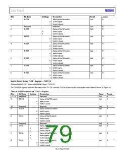
Switch Matrix Status Px/Pxx Register—PSWSTA
Address 0x000021B4, Reset: 0x00000000, Name: PSWSTA
The PSWSTA register indicates the status of the Px/Pxx switches. The bit names are the same as the switch names shown in Figure 33.
Table 88. Bit Descriptions for PSWSTA Register
Bits
[31:15]
14
Bit Name
Reserved
PL2STA
Settings
Description
Reserved.
Reset
0x0
0x0
Access
R
R
Status of PL2 switch.
Switch open.
Switch closed.
PL switch control.
Switch open.
0
1
13
PLSTA
0x0
R
0
1
Switch closed.
Rev. 0 | Page 77 of 130

 ADI [ ADI ]