AD5940
Data Sheet
PROGRAMMABLE SWITCH MATRIX
The AD5940 provides flexibility for connecting external pins
to the high speed DAC excitation amplifier and to the high
speed TIA inverting input. This flexibility supports options for
impedance measurements of different sensor types and allows
an ac signal to be coupled to the dc bias voltage of a sensor.
AFEx Switches
The AFE1, AFE2, and AFE3 switches are only intended for use
as switches. These switches are not ADC inputs. In a multi-
measurement system, these switches provide a method to switch
sensor electrodes, which is useful in bioelectric system applications.
When configuring the switches, take the switch settings on the
output of the low power amplifiers into account.
RECOMMENDED CONFIGURATION IN HIBERNATE
MODE
On power-up, all switches are open to disconnect the sensor.
To minimize leakage on the switches connecting to the positive
node and negative node of the excitation amplifier, and to
minimize leakage on the high speed TIA, it is recommended to
tie the switches to the internal 1.82 V LDO generated voltage by
closing the PL, PL2, NL, and NL2 switches.
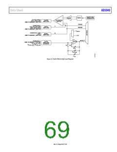
Figure 32 shows a high level diagram of how each of the switch
matrix nodes (data out, positive, negative, and TIA nodes)
connect to the internal circuitry of the AD5940. Figure 33
shows a detailed diagram of every switch on the matrix.
In hibernate mode, it is assumed that only the dc bias voltage
from the low power amplifiers is required for the sensor.
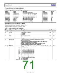
SWITCH DESCRIPTIONS
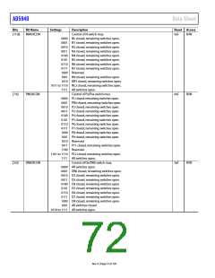
Dx/DR0 Switches
OPTIONS FOR CONTROLLING ALL SWITCHES
The Dx/DR0 switches select the pin to connect to the excitation
amplifier output of the high speed DAC. For an impedance
measurement, this pin is CE0. The output of the excitation
amplifier can be connected to an external calibration resistor
(RCAL) via the RCAL0 pin if the DR0 switch is closed.
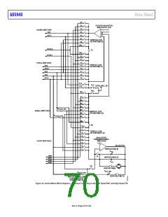
Figure 33 shows all switches connected to the high speed
DAC excitation amplifier and to the inverting input of the
high speed TIA.
Two options are available for controlling the switches on the
switch matrix,
Px/Pxx Switches
The Px/Pxx switches select the pin to connect to the positive node
of the excitation amplifier of the high speed DAC. For most
applications, this pin is RE0. The negative input of the excitation
amplifier can be connected to an external calibration resistor via
the RCAL0 pin if the PR0 switch is closed.
•
Control the Tx/TR1, Nx/Nxx, Px/Pxx, and Dx/DR0
switches as a group in the SWCON register.
Individual control of each switch within the switch matrix
using the xSWFULLCON registers.
•
If controlling the switches using the xSWFULLCON registers,
follow this sequence:
Nx/Nxx Switches
The Nx/Nxx switches select the pin to connect to the negative
node of the excitation amplifier of the high speed DAC. The
inverting input of the high speed TIA can be connected to an
external calibration resistor via the RCAL1 pin if the NR1
switch is closed.
1. Write to the specific bit in the xSWFULLCON register.
2. Set the SWSOURCESEL bit in the SWCON register. If this
bit is not set after writing to the xSWFULLCON register,
the changes do not take effect.
In addition, status registers are available to read back the open
or closed status of each switch.
Tx/TR1 Switches
The Tx/TR1 switches select the pin to connect to the inverting
input of the high speed TIA. The inverting input of the high
speed TIA can be connected to RCAL via the RCAL1 pin if the
TR1 switch is closed.
Rev. 0 | Page 68 of 130

 ADI [ ADI ]