AD5940
Data Sheet
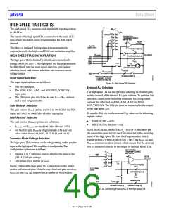
HIGH SPEED TIA CIRCUITS
The high speed TIA measures wide bandwidth input signals up
to 200 kHz.
N6
NL
TR1
HIGH SPEED
T1
T2
The output of the high speed TIA is connected to the main ADC
mux, where this output can be programmed as the ADC input
channel.
TRANSIMPEDANCE
AMPLIFIER
HSTIA
OUTPUT
T3
T4
T5
+
–
Tx/TR1
SWITCHES
This block is designed for impedance measurements in
conjunction with the high speed DAC and excitation amplifier.
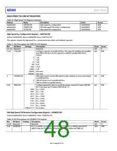
HSRTIACON[3:0]
R
TIA
R
TIA INPUT
LOAD02
T9
HSRTIACON[12:5]
HIGH SPEED TIA CONFIGURATION
SE0
AIN0
AIN1
AIN2
The high speed TIA is disabled by default and is turned on by
setting AFECON [11] = 1. The high speed TIA has programmable
flexibility built into the input signal selection, gain resistor
selection, input load resistor selection, and common-mode
voltage source.
C
TIA
SW6
T10
AIN4
HSRTIACON[4]
TIA_DE0
R
R
LOAD_DE0
DE0
DE0RESCON[7:0]
SWITCH AND RLOAD
CONTROLLED BY
DE0RESCON[7:0]
Input Signal Selection
The input signal options are as follows:
Figure 25. High Speed TIA Switches
The SE0 input pin.
The AIN0, AIN1, AIN2, and AIN3/BUF_VREF1V8
input pins.
The DE0 input pin, which has its own RLOAD/RTIA options
and is user programmable.
External RTIA Selection
The high speed TIA has the option of selecting an external gain
resistor instead of the internal RTIA gain options. To perform this
selection, connect one end of the resistor to the DE0 pin and
connect the other end to AIN0, AIN1, AIN2, or AIN3/
BUF_VREF1V8. The DE0 pin must be connected to the output
of the high speed TIA.
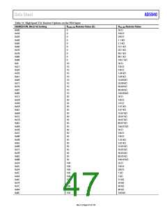
Gain Resistor Selection
The gain resistor (RTIA) options are 50 Ω to 160 kΩ for the DE0
input, and 200 Ω to 160 kΩ for all other input pins.
To use the DE0 pin for the external RTIA value, set the following
register values:
Load Resistor Selection
DE0RESCON = 0x97.
HSRTIACON, Bits[3:0] = 0xF.
The load resistor (RLOAD) options are as follows:
RLOAD02 and RLOAD04 are fixed 100 Ω for SE0 and AFE3.
For the DE0 pin, RLOAD is programmable. The user can
select values from 0 Ω, 10 Ω, 30 Ω, 50 Ω, and 100 Ω.
AIN0, AIN1, AIN2, or AIN3/BUF_VREF1V8 (whichever pin
the resistor is connected to) must be connected to the inverting
input of the high speed TIA (see the Programmable Switch
Matrix section). When DE0RESCON = 0x97, the RLOAD_DE0 and
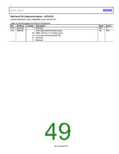
Common-Mode Voltage Selection
The high speed TIA common-mode voltage setting, on the positive
input to the high speed TIA amplifier, is configurable. The
configuration options are as follows:
R
R
TIA_DE0 resistors are short circuit, which means that the external
TIA is connected directly to the output of the high speed TIA.
HIGH SPEED
TRANSIMPEDANCE
AMPLIFIER
T1
Internal 1.11 V reference source, which is the same as the
VBIAS_CAP pin voltage.
AIN1
T2
HSTIA
OUTPUT
+
T3
Low power DAC output (VZERO0).
T4
T5
–
T9
HSRTIACON[3:0]
Figure 25 shows the high speed TIA connections to the switch
matrix and external pins. Note the extra load and gain resistors,
R
TIA
EXTERNAL
RTIA
HSRTIACON[12:5]
RLOAD_DE0 and RTIA_DE0, respectively, available on the DE0 pin.
T10
C
TIA
DE0RESCON
R
DE0
LOAD_DE0
DE0RESCON[7:0]
DE0RESCON[7:0]
Figure 26. Connecting External RTIA to the High Speed TIA
Rev. 0 | Page 46 of 130

 ADI [ ADI ]