AD5940
Data Sheet
HIGH PERFORMANCE ADC CIRCUIT
The ADC uses a precision, low drift, factory calibrated 1.82 V
reference. An external reference source can also be connected to
the VREF_1V8 pin.
ADC CIRCUIT OVERVIEW
The AD5940 implements a 16-bit, 800 kSPS, multichannel SAR
ADC. The ADC operates from a 2.8 V to 3.6 V power supply. The
host microcontroller interfaces to the ADC via the sequencer or
directly through the SPI interface.
ADC conversions are triggered by writing directly to the ADC
control register via the SPI interface, or by writing to the ADC
control register via the sequencer.
An ultralow leakage switch matrix is used for sensor connection
and can also be used to multiplex multiple electronic measurement
devices to the same wearable electrodes.
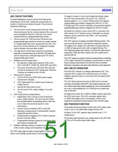
ADC CIRCUIT DIAGRAM
Figure 27 shows the ADC core architecture. Figure 27 excludes
input buffering, gain stages, and output postprocessing.
IN+
SWITCHES CONTROL
MSB
LSB
SW+
32,768C 16,384C
4C
4C
2C
2C
C
C
C
C
BUSY
REF
CONTROL
LOGIC
COMP
GND
OUTPUT CODE
32,768C 16,384C
MSB
LSB
SW–
CNV
IN–
Figure 27. ADC Core Block Diagram (IN+, REF, GND, and IN− are Internal Nodes)
V
ZERO
+
LPTIA0
–
SE0
AIN4/
LPF0
R
LPF
R
+
TIA
FRONT‐END
ADC
BUFFER
PREBUFFER
GAIN = 1/1.5/2/4/9
PGA
HSTIA
–
+
–
+
–
16-BIT ADC
800kSPS/
1600kSPS
POSTPROCESSING BLOCKS:
OFFSET/GAIN CALIBRATION,
DIGITAL FILTERS (SINC3/SINC2)
SECOND-
ORDER
ANTIALIAS
FILTER
R
TIA
–
+
–
+
VOLTAGE INPUTS:
AIN0 TO AIN6
VOLTAGE INPUTS:
DE0, SE0, CE0, RE0, V
,
ZERO0
V
BIAS0
VOLTAGE INPUTS:
HIGH SPEED DAC
EXCITATION AMP,
POSITIVE AND
NEGATIVE NODES
VOLTAGE INPUTS:
INTERNAL CHANNELS:
TEMP SENSORS,
INTERNAL VREFERENCES
POWER SUPPLY VOLTAGES
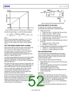
Figure 28. Basic Diagram of ADC Input Channel
Rev. 0 | Page 50 of 130

 ADI [ ADI ]