AD5940
Data Sheet
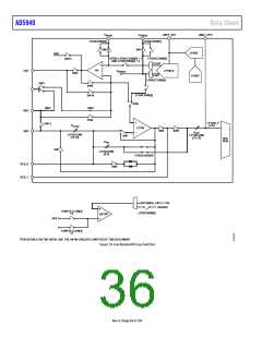
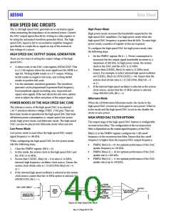
HIGH SPEED DAC CIRCUITS
The 12-bit high speed DAC generates an ac excitation signal
when measuring the impedance of an external sensor. Control
the DAC output signal directly by writing to a data register or
by using the automated waveform generator block. The high
speed DAC signal is fed to an excitation amplifier designed
specifically to couple the ac signal on top of the normal dc
bias voltage of a sensor.
High Power Mode
High power mode increases the bandwidth supported by the
high speed DAC amplifiers. Use high power mode when the
high speed DAC frequency is greater than 80 kHz. To enter high
power mode, a number of register writes are required.
To configure the high speed DAC for high power mode, take
the following steps:
HIGH SPEED DAC OUTPUT SIGNAL GENERATION
1. Set the PMBW register, Bit 0 = 1. Power consumption is
increased, but the output signal bandwidth increases to a
maximum of 200 kHz. In high power mode, the system
clock to the DAC and the ADC is 32 MHz.
2. Ensure that CLKSEL, Bits[1:0] select a 32 MHz clock
source. For example, to select internal high speed oscillator
set CLKSEL, Bits[1:0] (SYSCLKSEL) = 00. Ensure that the
system clock divide ratio is 1 (CLKCON0, Bits[5:0] = 0
or 1).
There are two ways of setting the output voltage of the high
speed DAC:
•
•
A direct write to the DAC code register, HSDACDAT. This
is a 12-bit register where the most significant bit (MSB) is a
sign bit. Writing 0x800 results in a 0 V output. Writing
0x200 results in negative full-scale, and writing 0xE00
results in positive full-scale.
Use the automatic waveform generator. The waveform
generator can be programmed to generate fixed frequency,
fixed amplitude signals including, sine, trapezoid and
square wave signals. If the user selects the sine wave, options
exist to adjust the offset and phase of the output signal.
3. If the internal high speed oscillator is selected as the system
clock source, ensure that the 32 MHz option is selected.
Clear HSOSCCON, Bit 2 = 0.
Hibernate Mode
When the AD5940 enters hibernate mode, the clocks to the
high speed DAC circuits are clock gated to save power. When in
active mode and the high speed DAC is not in use, disable the
clocks to save power.
POWER MODES OF THE HIGH SPEED DAC CORE
The reference source of the high speed DAC is an internal
1.82 V precision reference voltage (VREF_1V82 pin). There are
three basic modes of operation for the high speed DAC that trade
off between power consumption vs. output speed: low power
mode, high power mode, and hibernate mode. The high speed
DAC can also be placed into hibernate mode when inactive.
HIGH SPEED DAC FILTER OPTIONS
The output stage of the high speed DAC features a configurable
reconstruction filter. The configuration of the reconstruction
filter is dependent on the output signal frequency of the DAC.
Low Power Mode
Low power mode is used when the high speed DAC output
signal frequency is <80 kHz.
Bits[3:2] in the PMBW register configure the 3 dB cutoff
frequency of the reconstruction filter. Ensure that the cutoff
frequency is higher than the required DAC output frequency.
When configuring the high speed DAC for low power mode,
take the following steps:
•
•
•
PMBW, Bits[3:2] = 01 for optimal performance if the DAC
update frequency is ≤50 kHz.
PMBW, Bits[3:2] = 10 for optimal performance if the DAC
update rate is ≤100 kHz.
PMBW, Bits[3:2] = 11 for optimal performance if the DAC
update rate is up to 250 kHz.
1. Clear the PMBW register (Bit 0 = 0).
2. In this mode, the system clock to the high speed DAC and
the ADC is 16 MHz.
3. Ensure that CLKSEL, Bits[1:0] = 0 to select a 16 MHz,
internal, high frequency oscillator clock source. Ensure the
system clock divide ratio is 1 (CLKCON0, Bits[5:0] = 0
or 1.
4. If the internal high speed oscillator is selected as the system
clock source, ensure that the 16 MHz option is selected. Set
HSOSCCON, Bit 2 = 1.
V
FROM
BIAS
LOW POWER DAC
DAC CODE DIRECT
HIGH
OUTPUT
D
+
–
PROGRAMMABLE
GAIN
RECONSTRUCTION
FILTER
EXCITATION
AMPLIFIER
SPEED
DAC
AMPLIFIER
WAVEFORM
GENERATOR
V
FROM
ZERO
LOW POWER DAC
Figure 20. High Speed DAC Block
Rev. 0 | Page 40 of 130

 ADI [ ADI ]