Data Sheet
AD5940
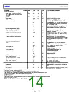
To calculate the rms bits, use the following equation:
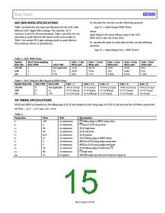
ADC RMS NOISE SPECIFICATIONS
log2 ((2 × Input Range)/RMS Noise)
Table 2 provides the rms noise specifications for the ADC with
different ADC digital filter settings. The internal 1.82 V
reference is used for all measurements. Table 3 provides the rms
and peak-to-peak effective bits based on the noise results in
Table 2 for various PGA gain settings (peak-to-peak effective
bits results are shown in parentheses).
where:
Input Range is the input voltage range to the ADC
RMS Noise is the rms of the noise.
To calculate the peak-to-peak effective bits, use the following
equation:
log2 ((2 × Input Range)/(6.6 × RMS Noise))
Table 2. ADC RMS Noise
Update
Rate (Hz)
Sinc3 Oversampling
Rate (OSR)
Gain = 1 rms
Noise (μV)
Gain = 1.5 rms
Noise (μV)
Gain = 2 rms
Noise (μV)
Gain = 4 rms
Noise (μV)
Gain = 9 rms
Noise (μV)
Sinc2 OSR
Not applicable
22
200,000
9090
900
4
4
5
72.43
29.29
24.0
49.732
19.59
17.11
37.83
10.4
12.832
18.93
6.687
6.416
8.62
4.42
1.018
178
Table 3. ADC Effective Bits Based on RMS Noise
Update Rate (Hz)
Sinc3 OSR Sinc2 OSR
Gain = 1
Gain = 1.5
Gain = 2
Gain = 4
Gain = 9
200,000
9090
900
4
4
5
Not applicable
22
178
14.6 (11.9 p-p)
15 (13.18 p-p)
15 (13.47 p-p)
15 (12.4 p-p)
15 (13.8 p-p)
15 (13.96 p-p) 15 (13.8 p-p)
14.95 (12.23 p-p)
15 (14.09 p-p)
14.95 (12.23 p-p)
15 (13.73 p-p)
15 (13.79 p-p)
14.9 (12.15 p-p)
15 (13.15 p-p)
15 (15 p-p)
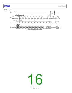
SPI TIMING SPECIFICATIONS
MOSI and MISO are launched on the falling edge of SCLK and sampled on the rising edge of SCLK by the host and the AD5940, respectively.
IOVDD = 2.8 V − 3.6 V and 1.8V 10 ꢀ
Table 4.
Parameter
Time
190
5
Unit
Description
t1
ns maximum
ns minimum
ns minimum
ns minimum
ns minimum
ns maximum
ns minimum
ns minimum
ns minimum
ns minimum
μs typical
CS falling edge to MISO setup time
CS low to SCLK setup time
SCLK high time
SCLK low time
SCLK period
SCLK falling edge to MISO delay
MOSI to SCLK rising edge setup time
MOSI to SCLK rising edge hold time
SCLK falling edge to hold time CS
CS high time
t2
t3
t4
t5
t6
t7
t8
t9
40
40
62.5
27
5
5
19
80
22
t10
tWK
AD5940 wake-up time (not shown in Figure 3)
Rev. 0 | Page 15 of 130

 ADI [ ADI ]