AD5940
Data Sheet
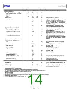
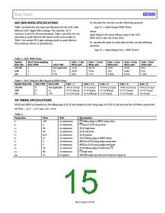
Parameter
Symbol Min
Typ
Max
Unit
Test Conditions/Comments
POWER REQUIREMENTS
Power Supply Voltage Range (AVDD
to AGND, DVDD to DGND, and IOVDD
to DGND)
2.8
3.3
3.6
V
IOVDD9
1.62
1.8
0.56
8.5
1.98
0.74
V
mA
μA
AVDD Current
Hibernate Mode
Analog peripheral in idle mode
Only low power DAC, PAs, low power reference,
low power TIA and 32 kHz oscillator active
6.5
1.8
μA
μA
Only low power DACs, PA, low power reference,
and 32 kHz oscillator active; PA and low power
TIA in half power mode
Lowest power mode; only wake-up timer
active; all analog peripherals powered down
Impedance Measurement Modes
Impedance Spectroscopy Mode
9.1
mA
μA
When ac impedance engine, ADC and
sequencer are active
50 kHz excitation signal; DFT enabled with DFT
sample number = 2048; 1 Hz output data rate
(ODR)
When low power loop creates sine wave at
100 Hz and the receive channel and DFT engineis
duty cycled, with DFT sample number = 16, gives
4 Hz ODR
50 kHz Impedance Measurement
100 Hz Impedance Measurement
106
65
μA
Additional Power Supply Currents
ADC
1.5
mA
ADC frequency (fADC) = 200 kSPS, ADC clock is
16 MHz
3.45
0.3
0.9
mA
mA
fADC = 400 kSPS, ADC clock is 32 MHz
Low power mode
High power mode
Includes excitation amplifier and
instrumentation amplifier
High Speed TIA
High Speed DAC
2.2
4.5
550
1.65
2.3
mA
mA
μA
μA
μA
Low power mode
High power mode
DFT Hardware Accelerator
Low Power Reference
Low Power DACs for VZERO0 and VBIAS0
Low power DAC powered up, excluding load
current
Low Power TIA and PA
2
1
μA
μA
Per amplifier, normal mode
Per amplifier, half power mode
Processor clock = 16 MHz
Wake-up time to allow communication on SPI
bus
START-UP TIME
AFE Wake-Up
30
80
ms
μs
ADC Wake-Up1
180
Time delay required on exiting hibernate mode
before starting ADC conversions
1 Guaranteed by design, not production tested.
2 Code distribution can be reduced if ADC output rate is reduced by using sinc2 filter option.
3 ADC offset and gain not calibrated for high power mode in production. User calibration can eliminate this error.
4 Noise can be reduced if ADC sample rate is reduced using the sinc2 filter.
5 See Figure 6 for details.
6 See Figure 8 for details.
7 High speed DAC offset calibration can remove this error. See the High Speed DAC Calibration Options section for details.
8 Measured using the box method
9 IOVDD can optionally be powered from a 1.8 V supply rail.
Rev. 0 | Page 14 of 130

 ADI [ ADI ]