Data Sheet
AD5940
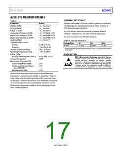
ABSOLUTE MAXIMUM RATINGS
THERMAL RESISTANCE
Table 5.
Thermal performance is directly linked to printed circuit board
(PCB) design and operating environment. Close attention to
PCB thermal design is required.
Parameter
Rating
AVDD to AGND
DVDD to DGND
IOVDD to DGND
Analog Input Voltage to AGND
Digital Input Voltage to DGND
Digital Output Voltage to DGND
AGND to DGND
Total GPIOx Pins Current
Positive
−0.3 V to +3.6 V
−0.3 V to +3.6 V
−0.3 V to +3.6 V
−0.3 V to AVDD +0.3V
−0.3 V to DVDD +0.3V
−0.3 V to DVDD +0.3V
−0.3 V to +0.3 V
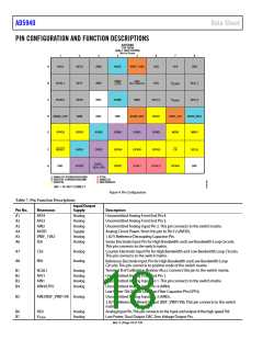
θJA is the natural convection junction to ambient thermal
resistance measured in a one cubic foot sealed enclosure.
θJC is the junction to case thermal resistance.
Table 6. Thermal Resistance1
Package Type
θJA
θJC
Unit
0 mA to 30 mA
−30 mA to 0 mA
−65°C to +150°C
−40°C to +85°C
CB-56-3
33.0702
0.0642
°C/W
Negative
1 Thermal impedance simulated values are based on a JEDEC 2S2P thermal test board. See
JEDEC JESD51.
Storage Temperature Range
Operating Temperature Range
Reflow Profile
Moisture Sensitivity Level 3 (MSL3)
Junction Temperature
Electrostatic Discharge (ESD)
Human Body Model (HBM)
ESD CAUTION
J-STD 020E (JEDEC)
150°C
2 kV
1 kV
Field Induced Charged Device
Model (FICDM)
Machine Model (MM)
100 V
Stresses at or above those listed under Absolute Maximum
Ratings may cause permanent damage to the product. This is a
stress rating only; functional operation of the product at these
or any other conditions above those indicated in the operational
section of this specification is not implied. Operation beyond
the maximum operating conditions for extended periods may
affect product reliability.
Rev. 0 | Page 17 of 130

 ADI [ ADI ]