Data Sheet
AD5940
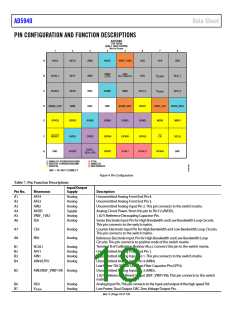
Input/Output
Supply
Pin No.
Mnemonic
Description
B8
RC0_1
Analog
Low Power TIA Reconstruction Filter 0 Feedback Pin 1. This pin is connected to the
output of the low power TIA.
C1
C2
C3, D3
C4
C5
C6
C7
C8
RCAL0
AFE2
DNC
AGND
AIN6
RC0_2
VBIAS0
Analog
Analog
Analog
Ground
Analog
Analog
Analog
Analog
Terminal A of Calibration Resistor. Connect this pin to the switch matrix.
Uncommitted Analog Front End Pin 2.
Do Not Connect. Do not connect to this pin.
Analog Ground. Short this pin to Pin E3 (AGND).
Uncommitted Analog Input Pin 6.
Low Power TIA Reconstruction Filter 0 Pin 2. This pin can be left open (optional).
Low Power, Dual-Output DAC Bias Voltage Output Pin.
Low Power TIA Feedback Pin. This pin is connected to the feedback of the low
power TIA.
RC0_0
D1
D2
VBIAS_CAP
AIN0
Analog
Analog
Not applicable
Ground
Digital
VBIAS0 Decoupling Capacitor Pin.
Uncommitted Analog Input Pin 0. This pin connects to the switch matrix.
Do Not Connect. Do not connect to this pin.
Analog Reference Ground.
D4, G1, G8 DNC
D5
D6
AGND_REF
GPIO1
General-Purpose Input/Output Pin 1.
input/output
D7
D8
E1
VREF_2V5
AVDD_REG
GPIO2
Analog
Supply
Digital
2.5 V Analog Reference Decoupling Capacitor Pin.
Analog Regulator Decoupling Capacitor Pin.
General-Purpose Input/Output Pin 2.
input/output
E2
GPIO3
Digital
General-Purpose Input/Output Pin 3.
input/output
E3
E4 to E6
E7
E8
F1
AGND
DGND
MOSI
Ground
Ground
Digital input
Digital output
Digital input
Supply
Analog Ground. Short this pin to Pin C4.
Digital Ground
SPI Master Output, Slave Input.
SPI Master Input Slave Output.
Reset Pin, Active Low.
MISO
RESET
AVDD
DVDD
GPIO6
F2
F3
F4
Analog 3.3 V Circuit Power.
Digital Circuit Power.
General-Purpose Input/Output Pin 6.
Supply
Digital
input/output
F5
F6
F7
GPIO0
GPIO5
CS
Digital
input/output
Digital
input/output
General-Purpose Input/Output Pin 0.
General-Purpose Input/Output Pin 5.
SPI Chip Select.
Digital
input/output
F8
SCLK
IOVDD
DVDD_REG_1V8
GPIO7
Digital input
Supply
Analog
SPI Clock.
G2
G3
G4
Digital Input/Output Supply Pin. DVDD (Pin F3) must be driven before IOVDD is enabled.
1.8 V Digital Regulator Decoupling Capacitor Pin.
General-Purpose Input/Output Pin 7.
Digital
input/output
G5
G6
G7
XTALI
XTALO
GPIO4
Digital Input
Digital Output
Digital
16 MHz External Crystal Input Pin.
16 MHz External Crystal Output Pin.
General-Purpose Input/Output Pin 4.
input/output
Rev. 0 | Page 19 of 130

 ADI [ ADI ]