AD5940
Data Sheet
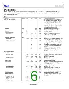
Parameter
Symbol Min
Typ
Max
Unit
Test Conditions/Comments
Input Common-Mode Range1
300
AVDD − mV
700
AVDD − mV
400
Output Voltage Range1
200
Overcurrent Limit Protection1
17
mA
Amplifier attempts to limit the source/sink
current to this value via the internal clamp;
tested with RLOAD = 0 Ω and RTIA = 100 Ω
Allowed Duration of Overcurrent
Limit1
Allowed Frequency of Overcurrent
Conditions
5
1
sec
Per hour
Short-Circuit Protection
12
mA
V
When amplifier output is shorted to ground
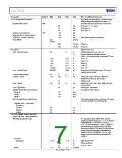
LOW POWER, ON-CHIP VOLTAGE
REFERENCE
2.5
0.47 µF from VREF_2V5 to AGND; reference is
measured with low power voltage DAC and
output amplifier enabled
Accuracy
5
mV
µV p-p
ppm/°C
TA = 25°C
Noise1
60
10
Reference Temperature Coefficient1, 8
−25
+25
PSRR
DC
AC5
70
48
dB
dB
AC 1 kHz; 50 mV p-p ripple applied to AVDD
supply
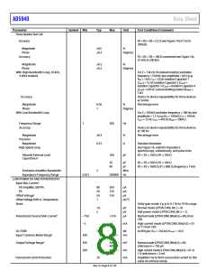
HIGH POWER, ON-CHIP VOLTAGE
REFERENCE
Accuracy
Reference Temperature Coefficient1
1.82
5
V
0.47 µF from VREF_1V82 to AGND; reference is
measured with ADC enabled
TA = 25 °C
5
+20
mV
ppm/°C
−20
PSRR
DC6
AC
85
60
dB
dB
DC; variation due to AVDD supply changes
AC; 1 kHz, 50 mV p-p ripple applied to AVDD
supply
ADC Common-Mode Reference Source
1.11
V
470 nF from bias capacitor on ADC (VBIAS_CAP)
to AGND; reference is measured with ADC
enabled
Accuracy
5
mV
TA = 25°C
Reference Temperature Coefficient1
DC Power Supply Rejection Ratio
AC Power Supply Rejection Ratio
−20
PSRR
PSRR
+20
ppm/°C
dB
dB
80
60
DC variation due to AVDD supply changes
AC 1 kHz, 50 mV p-p ripple applied to AVDD
supply
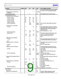
LOW POWER, DUAL OUTPUT DAC
VBIAS0 specifications derived from
(VBIAS0 AND VZERO0
)
measurements taken with potentiostat in
unity-gain mode and measured at CE0; VZERO0
specifications derived from measurements at
VZERO0; dual output low power DAC
Resolution1
12-Bit Mode
6-Bit Mode
Number of data bits
12
6
Bits
Bits
Relative Accuracy1
INL
12-Bit Mode
6-Bit Mode
−3.5
−3.5
1
0.5
+3
+2
LSB
LSB
1 LSB = 2.2 V/(212 − 1)
1 LSB = 2.2 V/26
Differential Nonlinearity1
12-Bit Mode
6-Bit Mode
Offset Error1
DNL
−0.99
−0.5
−7
+2.5
+0.5
+7
LSB
LSB
mV
Guaranteed monotonic, 1 LSB = 2.2 V/(212 − 1)
Guaranteed monotonic, 1 LSB = 2.2 V/26
VBIAS0/VZERO0 in 12-bit mode; 2.5 V internal
reference, DAC output code = 0x000; Target
0x000 code = 200 mV
3.9
−2
0.2
5
+2.6
mV
Differential offset voltage of VBIAS0 referred to
VZERO0
VBIAS0 or VZERO0 referred to AGND
Drift
µV/°C
Rev. 0 | Page 10 of 130

 ADI [ ADI ]