AD5940
Data Sheet
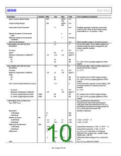
SPECIFICATIONS
AVDD = DVDD = 2.8 V to 3.6 V; the maximum difference between supplies = 0.3 V; IOVDD = 1.8 V 10% and 2.8 V to 3.6 V; the ADC
reference, excitation, DAC, and amplifier = 1.82 V, internal reference; low power DAC reference = 2.5 V, internal reference; TA = −40°C to
+85°C, unless otherwise noted.
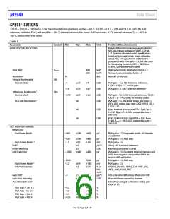
Table 1.
Parameter
Symbol Min
Typ
Max
Unit
Test Conditions/Comments
BASIC ADC SPECIFICATIONS
Pseudo differential mode measured relative to
ADC bias voltage (voltage on VBIAS_CAP pin,
1.11 V), unless otherwise noted; specifications
based on high speed mode, unless otherwise
noted; ADC voltage channel calibrated in
production with PGA gain = 1.5; AFE die clock
for the analog domain (ACLK) = 32 MHz or
16 MHz, unless otherwise noted
High speed mode; decimation factor = 4
Normal mode; decimation factor = 4
Number of data bits
Data Rate1
fSAMPLE
400
200
kSPS
kSPS
Bits
Resolution1
16
Integral Nonlinearity1
Normal Mode
INL
−4
2.0
2.0
+4
LSB
LSB
PGA gain = 1.5, 1.82 V internal reference,
1 LSB = 1.82 V ÷ 215 ÷ PGA gain
PGA gain = 9, 1.82 V internal reference
−5.6
DNL
+4.7
Differential Nonlinearity1
Normal Mode
−0.99
0.9
6
+2.5
LSB
LSB
PGA gain = 1.5, 1.82 V internal reference; 1 LSB =
1.82 V ÷ 215 ÷ PGA gain, no missing codes
PGA gain = 1.5, low power mode, ADC input =
0.9 V; ADC output data rate = 200 kSPS; 1 LSB =
1.82 V ÷ 215
DC Code Distribution2
6
6
LSB
LSB
Input channel is low power TIA = 1 µA, RTIA =
512 kΩ, RLOAD = 10 Ω ADC output data rate =
200 kSPS
Input channel is high speed TIA = 1 µA, RTIA
=
10 kΩ, RLOAD = 100 Ω ADC output data rate =
200 kSPS
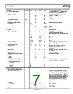
ADC ENDPOINT ERRORS
Offset Error
Low Power Mode
−600
200
+600
µV
PGA gain = 1.5, low power mode, all channels
except AIN3
−620
−1.1
200
0.5
3
2
400
+880
+1.4
µV
PGA gain = 1.5, AIN3 only
PGA gain = 1.5
Using 1.82 V internal reference
Matching compared to AIN3
PGA gain = 1.5, Excluding internal channels and
AIN3; both negative and positive full scale;
error at both endpoints
3
High Power Mode1,
mV
µV/°C
LSB
µV
Drift1
Offset Matching
Full-Scale Error
−1000
+800
-1000
−2.2
1000
+1.82
0.751
µV
mV
% of
full-
PGA gain = 1.5. AIN3 only
PGA gain = 1.5
AVDD/2, DVDD/2, VBIAS_CAP, VREF_2V5,
VREF_1V82, AVDD_REG
High Power Mode1,3
Internal Channels
0.9
0.21
scale
µV/°C
LSB
Gain Drift1
Gain Error Matching
PGA Mismatch Error1
−3
1
3
+3
Full-scale error drift minus offset error drift
Mismatch from channel to channel
ADC offset and gain calibration with a gain
value of 1.5
PGA Gain = 1 to 1.5
PGA Gain =1.5 to 2
PGA Gain = 2 to 4
PGA Gain = 4 to 9
−0.2
−0.2
−0.3
−0.55
+0.1
+0.1
+0.2
+0.2
+0.3
+0.3
+0.8
+0.55
%
%
%
%
Rev. 0 | Page 6 of 130

 ADI [ ADI ]