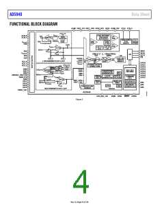
AD5940
Data Sheet
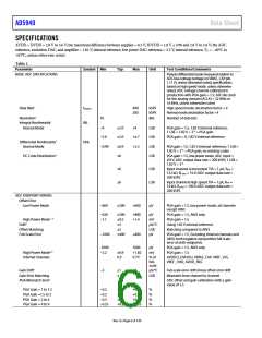
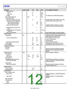
Parameter
Symbol Min
Typ
Max
Unit
Test Conditions/Comments
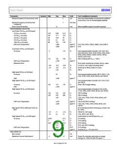
Three-Resistor Star Cell
Accuracy
R1 = R2 = R3 = 2.2 Ω (see Figure 14); 0.1 Hz to
200 kHz
Magnitude
Phase
0.ꢀ
0.ꢀ
%
Degrees
Accuracy
R1 = R2 = R3 = 100 Ω connected (see Figure 14);
0.1 kHz to 200 kHz
Magnitude
Phase
0.2
0.2
%
Degrees
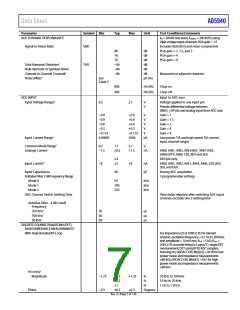
With High Bandwidth Loop, ꢀ0 kHz,
4-Wire Isolated
For Z = 1 kΩ (0.1% tolerant resistor); excitation
frequency = ꢀ0 kHz; sine amplitude = 0.6 V p-p;
RTIA = 1 kΩ; CTIA = 32 pF; Isolation Capacitor 1
(CISO1) = 1ꢀ nF; Isolation Capacitor 2 (CISO2) =
Isolation Capacitor 3 (CISO3) = Isolation Capacitor 4
(CISO4) = 470 nF; current-limiting resistor (RLIMIT) =
1 kΩ
Accuracy
Device to device repeatability for three devices
at ꢀ0 kHz
Magnitude
Phase
0.26
1
%
Percentage error
Degrees
With Low Bandwidth Loop
For Z = 100 kΩ; excitation frequency = 100 Hz; sine
amplitude = 1.1 V p-p; RTIA = 100 kΩ; CTIA = 100 nF;
CISO1 = 1ꢀ nF; CISO2 = 470 nF; RLIMIT = 1000 Ω
Frequency Range
Accuracy
1
300
Hz
Device to device repeatability for three devices
at 100 Hz
Magnitude
Precision
Magnitude
0.3
%
Ω
Percentage error
6.ꢀ3
Standard deviation
High Speed Loop
See Figure 14; valid for impedance
spectroscopy, voltammetry, and pulse tests
Allowed External Load
Capacitance1
100
pF
R2 + R3 ≤ 100 Ω; R1 ≤ 100 Ω
ꢀ0
40
pF
pF
R2 + R3 ≤ ꢀ00 Ω; R1 ≤ 100 Ω
R2 + R3 ≤ 1600 Ω; R1 ≤ 800 Ω; frequency ≥ 1 kHz
Excitation Amplifier Bandwidth
Impedance Frequency Range
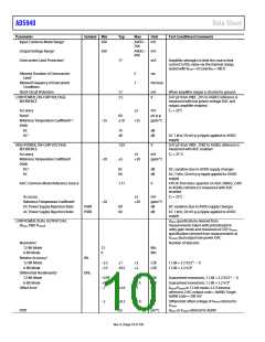
LOW POWER TIA AND POTENTIOSTAT
Input Bias Current1
3
MHz
200000 Hz
0.01ꢀ
TIA Amplifier, SE0 Pin
80
20
ꢀ0
1
200
1ꢀ0
1ꢀ0
pA
pA
μV
μV/°C
PA
Offset Voltage1
Offset Voltage Drift vs. Temperature
Noise
Unity-gain mode; V p-p in 0.1 Hz to 10 Hz range
Normal mode (LPTIACON0, Bit 2 = 0)
Half power mode (LPTIACON0, Bit 2 = 1)
Normal mode (LPTIACON0, Bits[4:3] = 00); from
CE0
High current mode (LPTIACON0, Bits[4:3] = 01
or 11 from CE0
1.6
2
μV
μV
μA
Potentiostat Source/Sink Current1
−7ꢀ0
−3
+7ꢀ0
+3
mA
DC PSRR
70
dB
At RE0 pin; RTIA = 2ꢀ6 kΩ; RLOAD = 10 Ω
Input Common-Mode Range1
300
300
300
AVDD – mV
600
AVDD – mV
400
AVDD − mV
400
Output Voltage Range1
Normal mode (LPTIACON0, Bits[4:3] = 00;
sink/source = 7ꢀ0 μA
High current mode (LPTIACON0, Bits[4:3] = 01 or
11); sink/source = 3 mA
Overcurrent Limit Protection
20
mA
Amplifiers try to limit source/sink current to this
value via internal clamp
Rev. 0 | Page 8 of 130

 ADI [ ADI ]