ADV7180
FIELD 1
1
622
623 624
2
3
4
5
6
7
8
9
10
11
23
24
625
OUTPUT
VIDEO
HS
OUTPUT
VS
OUTPUT
PVBEG[4:0] = 0x1
PVEND[4:0] = 0x4
FIELD
OUTPUT
PFTOG[4:0] = 0x6
FIELD 2
314
310
311
312
315
316
317
318
319
320
321
322
323
336
337
313
OUTPUT
VIDEO
HS
OUTPUT
VS
OUTPUT
PVBEG[4:0] = 0x1
PVEND[4:0] = 0x4
FIELD
OUTPUT
PFTOG[4:0] = 0x6
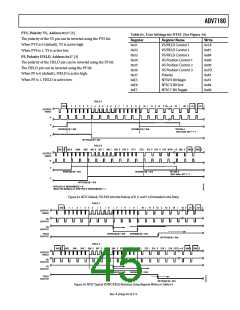
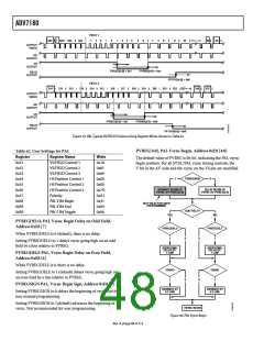
Figure 39. PAL Typical VS/FIELD Positions Using Register Writes Shown in Table 62
PVBEG[4:0], PAL Vsync Begin, Address 0xE8 [4:0]
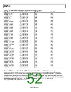
Table 62. User Settings for PAL
Register
0x31
0x32
0x33
0x34
0x35
0x36
0x37
0xE8
0xE9
0xEA
Register Name
VS/FIELD Control 1
VS/FIELD Control 2
VS/FIELD Control 3
HS Position Control 1
HS Position Control 2
HS Position Control 3
Polarity
Write
0x1A
0x81
0x84
0x00
0x00
0x7D
0xA1
0x41
0x84
0x06
The default value of PVBEG is 00101, indicating the PAL vsync
begin position. For all NTSC/PAL vsync timing controls, the
V bit in the AV code and the vsync on the VS pin are modified.
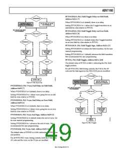
1
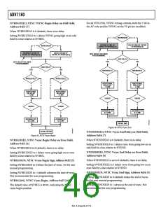
PVBEGSIGN
0
ADVANCE BEGIN OF
VSYNC BY PVBEG[4:0]
DELAY BEGIN OF
VSYNC BY PVBEG[4:0]
PAL V Bit Begin
NOT VALID FOR USER
PROGRAMMING
PAL V Bit End
ODD FIELD?
PAL F Bit Toggle
YES
NO
PVBEGDELO, PAL Vsync Begin Delay on Odd Field,
Address 0xE8 [7]
PVBEGDELO
1
PVBEGDELE
1
When PVBEGDELO is 0 (default), there is no delay.
0
0
Setting PVBEGDELO to 1 delays vsync going high on an odd
field by a line relative to PVBEG.
ADDITIONAL
DELAY BY
1 LINE
ADDITIONAL
DELAY BY
1 LINE
PVBEGDELE PAL, Vsync Begin Delay on Even Field,
Address 0xE8 [6]
When PVBEGDELE is 0, there is no delay.
VSBHO
1
VSBHE
1
Setting PVBEGDELE to 1 (default) delays vsync going high on
an even field by a line relative to PVBEG.
0
0
PVBEGSIGN PAL, Vsync Begin Sign, Address 0xE8 [5]
ADVANCE BY
0.5 LINE
ADVANCE BY
0.5 LINE
Setting PVBEGSIGN to 0 delays the beginning of vsync. Set for
user manual programming.
Setting PVBEGSIGN to 1(default) advances the beginning of
vsync. Not recommended for user programming.
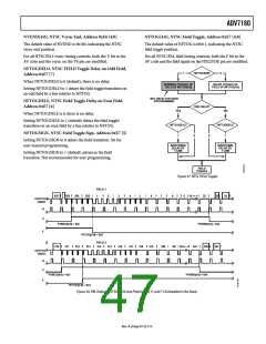
VSYNC BEGIN
Figure 40. PAL Vsync Begin
Rev. A | Page 48 of 112

 ADI [ ADI ]