ADV7180
PVS, Polarity VS, Address 0x37 [5]
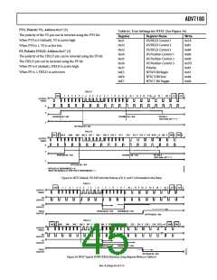
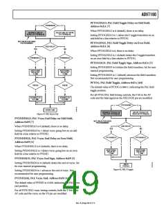
Table 61. User Settings for NTSC (See Figure 34)
The polarity of the VS pin can be inverted using the PVS bit.
When PVS is 0 (default), VS is active high.
When PVS is 1, VS is active low.
Register
0x31
0x32
0x33
0x34
0x35
0x36
0x37
0xE5
0xE6
0xE7
Register Name
Write
0x1A
0x81
0x84
0x00
0x00
0x7D
0xA1
0x41
0x84
0x06
VS/FIELD Control 1
VS/FIELD Control 2
VS/FIELD Control 3
HS Position Control 1
HS Position Control 2
HS Position Control 3
Polarity
PF, Polarity FIELD, Address 0x37 [3]
The polarity of the FIELD pin can be inverted using the PF bit.
The FIELD pin can be inverted using the PF bit.
When PF is 0 (default), FIELD is active high.
When PF is 1, FIELD is active low.
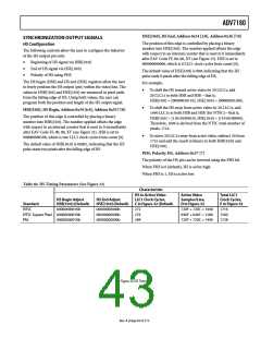
NTSV V Bit Begin
NTSC V Bit End
NTSC F Bit Toggle
FIELD 1
525
1
2
3
4
5
6
7
8
9
10
11
12
13
19
20
21
22
OUTPUT
VIDEO
H
V
1
NVBEG[4:0] = 0x5
NVEND[4:0] = 0x4
BT.656-4
REG 0x04, BIT 7 = 1
F
NFTOG[4:0] = 0x3
FIELD 2
262
263
264
265
266
267
268
269
270
271
272
273
274
275 276
283
284
285
OUTPUT
VIDEO
H
V
1
BT.656-4
REG 0x04, BIT 7 = 1
NVBEG[4:0] = 0x5
NVEND[4:0] = 0x4
F
NFTOG[4:0] = 0x3
APPLIES IF NEWAVMODE = 0:
1
MUST BE MANUALLY SHIFTED IF NEWAVMODE = 1.
Figure 33. NTSC Default, ITU-R BT.656 (the Polarity of H, V, and F is Embedded in the Data)
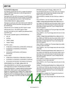
FIELD 1
525
1
2
3
4
5
6
7
8
9
10
11
12
13
14
15
21
22
OUTPUT
VIDEO
HS
OUTPUT
VS
OUTPUT
FIELD
NVBEG[4:0] = 0x0
NVEND[4:0] = 0x3
OUTPUT
NFTOG[4:0] = 0x5
FIELD 2
267
262
263
264
265
266
268
269
270
271
272
273
274
275
276 277
284
285
OUTPUT
VIDEO
HS
OUTPUT
VS
OUTPUT
NVBEG[4:0] = 0x0
NVEND[4:0] = 0x3
FIELD
OUTPUT
NFTOG[4:0] = 0x5
Figure 34. NTSC Typical VSYNC/FIELD Positions Using Register Writes in Table 61
Rev. A | Page 45 of 112

 ADI [ ADI ]