ADSP-BF542/ADSP-BF544/ADSP-BF547/ADSP-BF548/ADSP-BF549
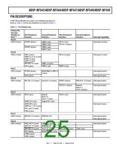
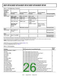
Table 11. Pin Multiplexing (Continued)
Primary Pin
Function
(Number of
First Peripheral
Function
Second Peripheral
Function
Third Peripheral
Function
Fourth Peripheral
Function
Pins)1, 2
Interrupt Capability
Port H
GPIO (14 pins)
UART1 (2 pins)
PPI0-1_FS3 (2 pins)
TMR8 (1 pin)
TACI1 (1 pin)
Interrupts (8 pins)
ATAPI_RESET (1 pin)
HOST_ADDR (1 pin)
PPI2_FS3 (1 pin)
TMR9 (1 pin)
Counter Down/Gate
(1 pin)
HOST_ACK (1 pin)
TMR10 (1 pin)
Counter Up/Dir
(1 pin)
MXVR MRX, MTX,
MRXON/GPW
(3 pins)4
DMAR 0–1 (2 pins)
TACI8–10 (3 pins)
TACLK8–10 (3 pins)
HWAITA
AMC Addr 4-9 (6 pins)
Interrupts (6 pins)
Port I
GPIO (16 pins)
Async Addr10–25
(16 pins)
Interrupts (8 pins)
Interrupts (8 pins)
Port J
GPIO (14 pins)
Async CTL and MISC
Interrupts (8 pins)
Interrupts (6 pins)
1 Port connections may be inputs or outputs after power up depending on the model and boot mode chosen.
2 All port connections always power up as inputs for some period of time and require resistive termination to a safe condition if used as outputs in the system.
3 A total of 32 interrupts at once are available from ports C through J, configurable in byte-wide blocks.
4 GPW functionality available when MXVR is not present or unused.
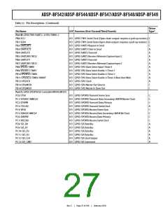
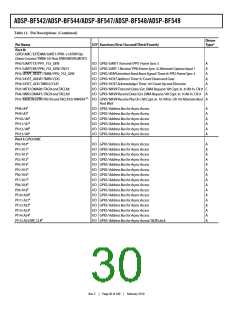
ADSP-BF54x processor pin definitions are listed in Table 12. To
see the pin multiplexing scheme, see Table 11.
Table 12. Pin Descriptions
Driver
Type2
Pin Name
I/O1 Function (First/Second/Third/Fourth)
Port A: GPIO/SPORT2–3/TMR4–7
PA0/ TFS2
PA1/ DT2SEC /TMR4
PA2/ DT2PRI
PA3/ TSCLK2
PA4/ RFS2
I/O GPIO/SPORT2 Transmit Frame Sync
I/O GPIO/SPORT2 Transmit Data Secondary/Timer 4
I/O GPIO/SPORT2 Transmit Data Primary
I/O GPIO/SPORT2 Transmit Serial Clock
I/O GPIO/SPORT2 Receive Frame Sync
C
C
C
A
C
C
C
A
C
C
C
A
C
C
C
PA5/ DR2SEC/TMR5
PA6/ DR2PRI
I/O GPIO/SPORT2 Receive Data Secondary/Timer 5
I/O GPIO/SPORT2 Receive Data Primary
PA7/ RSCLK2/TACLK0
PA8/ TFS3/TACLK1
PA9/ DT3SEC /TMR6
PA10/ DT3PRI /TACLK2
PA11/ TSCLK3/TACLK3
PA12/ RFS3/TACLK4
PA13/ DR3SEC/TMR7/TACLK5
PA14/ DR3PRI/TACLK6
PA15/ RSCLK3/TACLK7 and TACI7
I/O GPIO/SPORT2 Receive Serial Clock/Alternate Input Clock 0
I/O GPIO/SPORT3 Transmit Frame Sync/Alternate Input Clock 1
I/O GPIO/SPORT3 Transmit Data Secondary/Timer 6
I/O GPIO/SPORT3 Transmit Data Primary/Alternate Input Clock 2
I/O GPIO/SPORT3 Transmit Serial Clock/Alternate Input Clock 3
I/O GPIO/SPORT3 Receive Frame Sync/Alternate Input Clock 4
I/O GPIO/SPORT3 Receive Data Secondary/Timer 7/Alternate Input Clock 5
I/O GPIO/SPORT3 Receive Data Primary/Alternate Input Clock 6
I/O GPIO/SPORT3 Receive Serial Clock/Alt Input Clock 7 and Alt Capture Input 7 A
Rev. C
|
Page 26 of 100
|
February 2010

 ADI [ ADI ]