Data Sheet
ADM3055E/ADM3057E
INSULATION AND SAFETY RELATED SPECIFICATIONS
For additional information, see www.analog.com/icouplersafety.
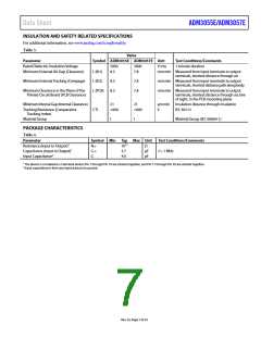
Table 3.
Value
Parameter
Symbol ADM3055E ADM3057E Unit
Test Conditions/Comments
1-minute duration
Rated Dielectric Insulation Voltage
Minimum External Air Gap (Clearance)
5000
8.3
3000
7.8
V rms
L (I01)
L (I02)
L (PCB)
mm min Measured from input terminals to output
terminals, shortest distance through air
Minimum External Tracking (Creepage)
8.3
8.3
7.8
7.8
mm min Measured from input terminals to output
terminals, shortest distance path along body
mm min Measured from input terminals to output
terminals, shortest distance through air, line
of sight, in the PCB mounting plane
Minimum Clearance in the Plane of the
Printed Circuit Board (PCB Clearance)
Minimum Internal Gap (Internal Clearance)
21
21
µm min Insulation distance through insulation
Tracking Resistance (Comparative
Tracking Index)
CTI
>600
>600
V
IEC 60112
Material Group
I
I
Material Group (IEC 60664-1)
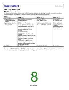
PACKAGE CHARACTERISTICS
Table 4.
Parameter
Symbol Min Typ Max Unit
Test Conditions/Comments
f = 1 MHz
Resistance (Input to Output)1
Capacitance (Input to Output)1
Input Capacitance2
RI-O
CI-O
CI
1013
3.7
4.0
Ω
pF
pF
1 The device is considered a 2-terminal device: Pin 1 through Pin 10 are shorted together, and Pin 11 through Pin 20 are shorted together.
2 Input capacitance is from any input data pin to ground.
Rev. A | Page 7 of 24

 ADI [ ADI ]