Data Sheet
ADM3055E/ADM3057E
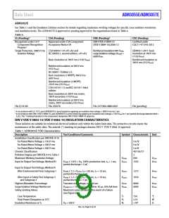
ABSOLUTE MAXIMUM RATINGS
Pin voltages with respect to GNDx are on the same side, unless
otherwise noted.
THERMAL RESISTANCE
Thermal performance is directly linked to PCB design and
operating environment. Careful attention to PCB thermal
design is required.
Table 9.
Parameter
Rating
θ
JA is specified for the worst-case conditions, that is, a device
VCC
VIO
−0.5 V to +6 V
−0.5 V to +6 V
−0.5 V to VIO + 0.5 V
soldered in a circuit board for surface-mount packages.
Logic Side Input/Output: TXD, RXD,
AUXIN, SILENT, STBY
CANH, CANL
Table 10. Thermal Resistance
Package Type1
RI-20-1
θJA
49
53
Unit
°C/W
°C/W
−40 V to +40 V
AUXOUT, RS
−0.5 V to VISOIN + 0.5 V
−40°C to +105°C
−65°C to +150°C
150°C
RW-20
Operating Temperature Range
Storage Temperature Range
Junction Temperature (TJ Maximum)
Power Dissipation
1 Thermocouple located at the center of the package underside, test
conducted on a 4-layer board with thin traces. See the Thermal Analysis
section for thermal model definitions.
(TJ maximum − TA)/θJA
Electrostatic Discharge (ESD)
IEC 61000-4-2, CANH/CANL
Across Isolation Barrier to GND1
Contact Discharge to GND2
Air Discharge to GND2
ESD CAUTION
8 kV
8 kV
15 kV
4 kV
Human Body Model (HBM),
All Pins, 1.5 kΩ, 100 pF
Moisture Sensitivity Level (MSL)
3
Stresses at or above those listed under Absolute Maximum
Ratings may cause permanent damage to the product. This is a
stress rating only; functional operation of the product at these
or any other conditions above those indicated in the operational
section of this specification is not implied. Operation beyond
the maximum operating conditions for extended periods may
affect product reliability.
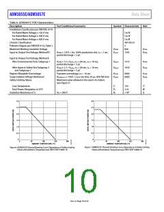
Table 11. Maximum Continuous Working Voltage1
Rating
Parameter
ADM3055E
ADM3057E
Unit
Constraint
AC Voltage
Bipolar Waveform
Basic Insulation
Reinforced Insulation
Unipolar Waveform
Basic Insulation
Reinforced Insulation
DC Voltage
566
467
566
467
VPEAK
VPEAK
Lifetime limited by insulation lifetime per VDE-0884-11
Lifetime limited by insulation lifetime per VDE-0884-11
1131
933
1131
933
VPEAK
VPEAK
Lifetime limited by insulation lifetime per VDE-0884-11
Lifetime limited by insulation lifetime per VDE-0884-11
Basic Insulation
Reinforced Insulation
1660
830
1560
780
VPEAK
VPEAK
Lifetime limited by package creepage per IEC 60664-1
Lifetime limited by package creepage per IEC 60664-1
1 Maximum continuous working voltage refers to the continuous voltage magnitude imposed across the isolation barrier. See the Insulation Lifetime section for more details.
Rev. A | Page 11 of 24

 ADI [ ADI ]