ADM3055E/ADM3057E
Data Sheet
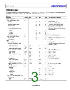
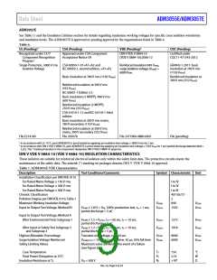
Parameter
Symbol Min
Typ Max
Unit
Test Conditions/Comments
Complementary Metal-Oxide
Semiconductor (CMOS) Logic
Input Currents
|IIH|, |IIL|
10
µA
Input high or low
RECEIVER
Differential Inputs
Differential Input Voltage Range
VID
See Figure 29, CRXD open,
−25 V < VCANL, VCANH < +25 V
Recessive
−1.0
+0.5
V
−1.0
+0.4
V
STBY high
Dominant
0.9
5.0
V
1.15
5.0
150
V
mV
µA
STBY high
Input Voltage Hysteresis
VHYS
Unpowered Input Leakage Current |IIN (OFF)
Input Resistance
|
10
VCANH, VCANL = 5 V, VCC = 0 V
CANH, CANL
Differential
Matching
RINH, RINL
RDIFF
mR
6
20
−0.03
25
100
+0.03
kΩ
kΩ
Ω/Ω
mR = 2 × (RINH − RINL)/(RINH + RINL)
Input Capacitance
CANH, CANL
Differential
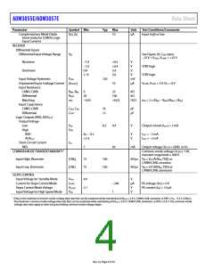
Logic Outputs (RXD, AUXOUT
Output Voltage
Low
High
RXD
AUXOUT
Short-Circuit Current
RXD
CINH, CINL
CDIFF
35
12
pF
pF
)
VOL
VOH
0.2
0.4
85
V
Output current (IOUT) = 2 mA
VIO − 0.2
+2.4
V
V
IOUT = −2 mA
IOUT = −2 mA
IOS
7
mA
Output voltage (VOUT) = GND1 or VIO
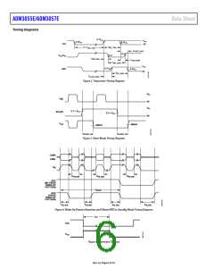
COMMON-MODE TRANSIENT IMMUNITY1
Common-mode voltage (VCM) ≥ 1 kV,
transient magnitude ≥ 800 V
Input High, Recessive
|CMH|
|CML|
75
75
100
100
kV/µs VIN = VIO (AUXIN, TXD) or
CANH/CANL recessive
kV/µs VIN = 0 V (AUXIN, TXD) or
CANH/CANL dominant
Input Low, Dominant
SLOPE CONTROL
Input Voltage for Standby Mode
Current for Slope Control Mode
Slope Control Mode Voltage
Input Voltage for High Speed Mode
VSTB
4.0
2.1
V
µA
V
ISLOPE
VSLOPE
VHS
−240
1
RS voltage (VRS) = 0 V
RS current (IRS) = 10 µA
V
1 |CMH| is the maximum common-mode voltage slew rate that can be sustained while maintaining AUXOUT ≥ 2.4 V, CANH/CANL recessive, or RXD ≥ VIO − 0.2 V. |CML| is
the maximum common-mode voltage slew rate that can be sustained while maintaining AUXOUT ≤ 0.4 V, CANH/CANL dominant, or RXD ≤ 0.4 V. The common-mode
voltage slew rates apply to both rising and falling common-mode voltage edges.
Rev. A | Page 4 of 24

 ADI [ ADI ]