ADG1419
PIN CONFIGURATION AND FUNCTION DESCRIPTIONS
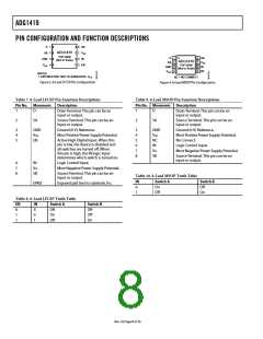
D
1
2
3
4
8
7
6
5
SB
ADG1419
TOP VIEW
(Not to Scale)
SA
V
SS
D
SA
1
2
3
4
8
7
6
5
SB
IN
GND
ADG1419
V
SS
EN
V
TOP VIEW
DD
GND
IN
(Not to Scale)
V
NC
DD
NOTES
1. EXPOSED PAD TIED TO SUBSTRATE, V
.
SS
NC = NO CONNECT
Figure 3. 8-Lead LFCSP Pin Configuration
Figure 4. 8-Lead MSOP Pin Configuration
Table 7. 8-Lead LFCSP Pin Function Descriptions
Table 9. 8-Lead MSOP Pin Function Descriptions
Pin No. Mnemonic
Description
Pin No. Mnemonic Description
1
D
Drain Terminal. This pin can be an
input or output.
1
D
Drain Terminal. This pin can be an
input or output.
2
SA
Source Terminal. This pin can be an
input or output.
2
SA
Source Terminal. This pin can be an
input or output.
3
4
5
GND
VDD
EN
Ground (0 V) Reference.
Most Positive Power Supply Potential.
Active High Digital Input. When this
pin is low, the device is disabled and
all switches are turned off. When
this pin is high, the IN logic input
determines which switch is turned on.
Logic Control Input.
Most Negative Power Supply Potential.
Source Terminal. This pin can be an
input or output.
Exposed pad tied to substrate, VSS.
3
4
5
6
±
8
GND
VDD
NC
IN
VSS
SB
Ground (0 V) Reference.
Most Positive Power Supply Potential.
No Connect.
Logic Control Input.
Most Negative Power Supply Potential.
Source Terminal. This pin can be an
input or output.
6
±
8
IN
VSS
SB
Table 10. 8-Lead MSOP Truth Table
IN
Switch A
Switch B
Off
EPAD
0
On
1
Off
On
Table 8. 8-Lead LFCSP Truth Table
EN
IN
Switch A
Switch B
Off
0
X
Off
1
0
On
Off
1
1
Off
On
Rev. 0 | Page 8 of 16

 ADI [ ADI ]